


1. Introduction
2. Experimental Method
2.1 Ag-Cu-Ti nano sputtering
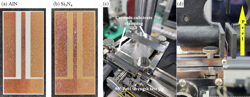
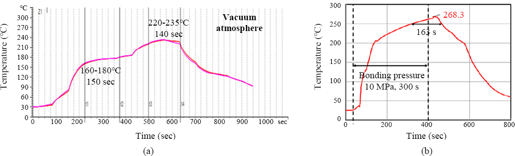
2.2 Ceramic/Cu brazing bonding
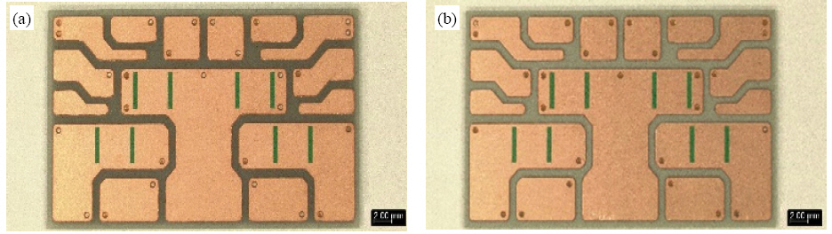
2.3 SiC device solder and sinter joints
2.4 Thermal shock test
3. Experiment Results
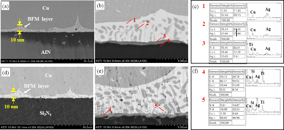
3.1 BFM (Brazing Filler Metal) surface microstructure analysis

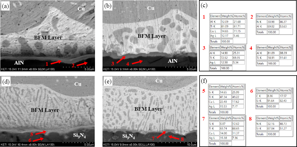
3.2 Analysis of brazing bonding characteristics
Fig.┬Ā5
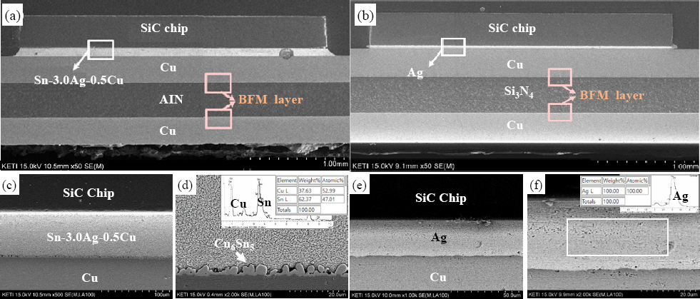
3.3 Analysis of solder and sinter joint microstructure
3.4 Analysis of brazing joint microstructure after the thermal shock test
Fig.┬Ā8

4. Conclusion
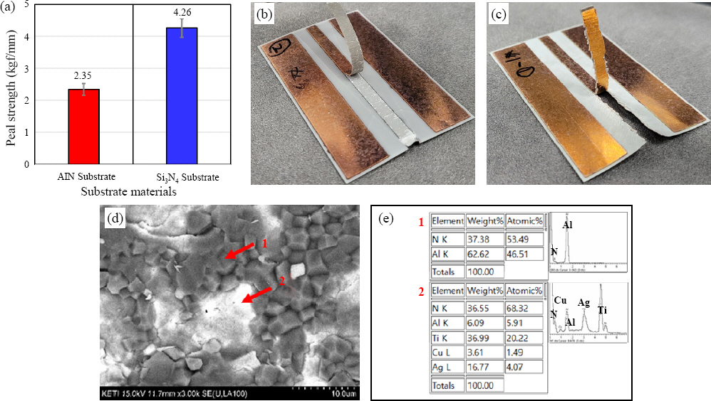
1) For the nano-sputtering thin film of Ag-Cu-Ti BFM, the surface roughness decreased under the 100 min condition compared to the 70 min condition, and the surface composition of the entire area was observed to be Ag-15.0Cu-2.3Ti.
2) After AMB bonding, the average thickness of the BFM layer was observed to be as low as approximately 10 ŃÄø. The peel strength of the ceramic/Cu interface was measured to be 2.35 kgf/mm for AlN and 4.26 kgf/mm for Si3N4. TiN compounds were observed at the AlN/BFM interface and the reaction layer estimated to be Ti5Si3 intermetallic compounds (IMCs) and TiN compounds at the Si3N4/BFM interface. This reaction layer appears to have affected the metal-ceramic bonding strength.
3) When cross-sectional microstructure analysis was conducted after SAC305 soldering and pressure Ag sintering bonding processes, it was observed that the Ag pressure sinter joint formed a very low thickness, and that the SiC device was well bonded without defects on both AlN and Si3N4 AMB substrates.
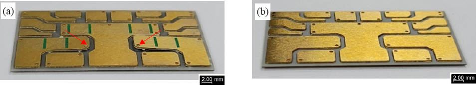
4) After the thermal shock test of 500 cycles under -55-150┬░C and 15 min dwell conditions, no defect was observed from the Si3N4 AMB substrate, but delamination was observed from the AlN substrate. Cross-sectional analysis confirmed that the fracture occurred in the TiN reaction layer of the AlN/BFM interface.
 PDF Links
 PubReader
 ePub Link
 Full text via DOI
 Download Citation
 Print
Print