


1. Introduction
2. Experimental Method
2.1 Test coupon preparation

2.2 Analysis of joint properties
2.2.1 Isothermal aging test
2.2.2 Microstructure and fracture surface analysis
Table┬Ā1
| Real peak temperature (┬░C) | 360 W | 380 W | 400 W |
|---|---|---|---|
| 1.5 s | 228 | 235 | 242 |
| 2.0 s | 228 | 235 | 243 |
| 2.5 s | 229 | 236 | 245 |
2.2.3 Low-speed shear test

3. Results and Discussion
Fig.┬Ā3

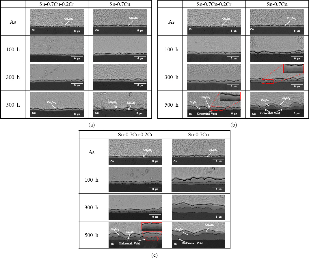
Fig.┬Ā5

Fig.┬Ā6

Fig.┬Ā7
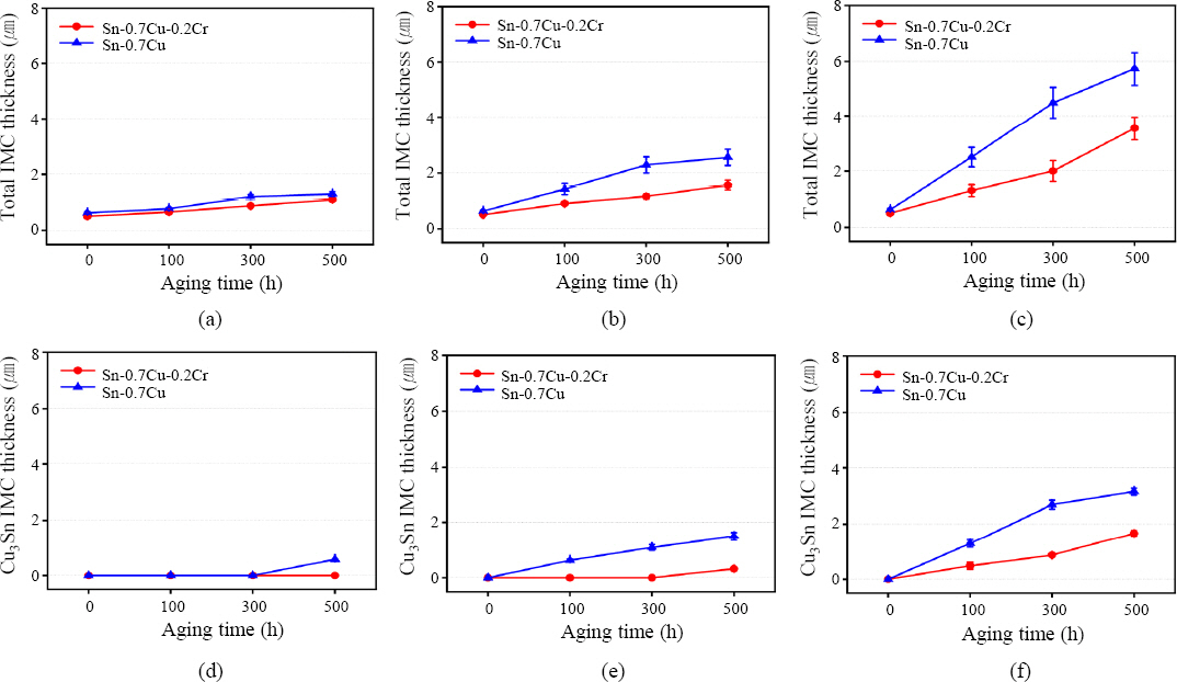
Fig.┬Ā8
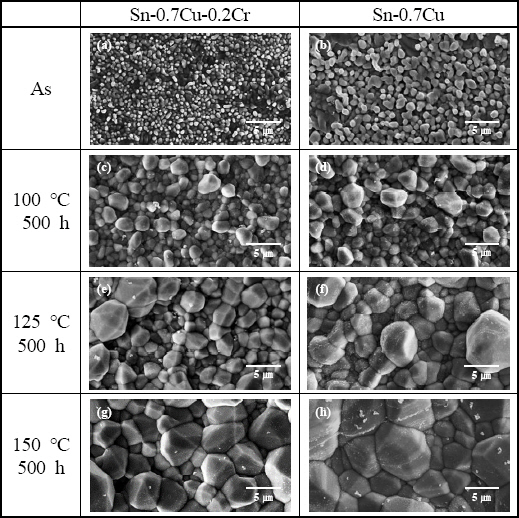
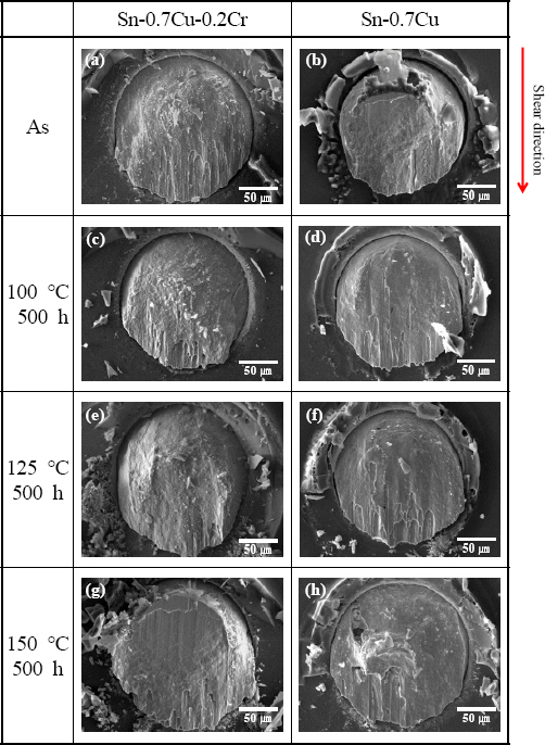
Fig.┬Ā9
4. Conclusions
1) When the microstructures of the solders were analyzed, both solders exhibited small grain sizes at the beginning. As isothermal aging progressed, coarsening of the grains and intermetallic compounds (IMCs) inside the solders was observed. In the solder containing Cr, however, the growth of grains and IMCs was inhibited.
2) When the IMC thickness was compared, the IMC thickness at the beginning and after isothermal aging was lower in the Sn-0.7Cu-0.2Cr solder compared to the Sn-0.7Cu solder. The Cu3Sn IMC and Kirkendall void were also less observed in the Sn-0.7Cu-0.2Cr solder.
3) When the IMC grain size was compared, the initial grain size of the Sn-0.7Cu-0.2Cr solder was found to be smaller. The IMCs and grains inside the solder after isothermal aging were also found to be smaller compared to the Sn-0.7Cu solder.
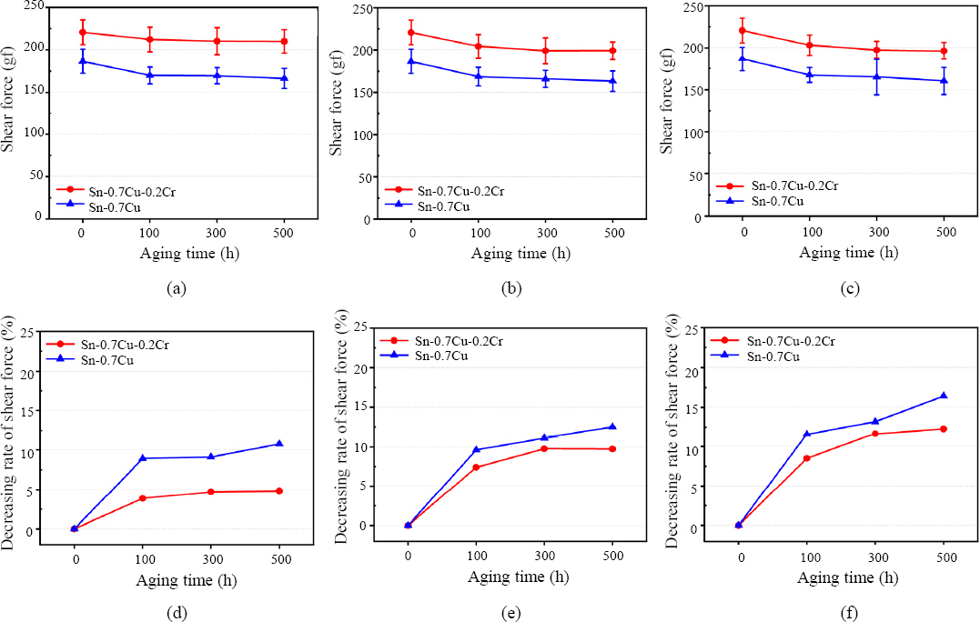
4) The bonding strength measurement results revealed that the initial shear force of the Sn-0.7Cu-0.2Cr solder was approximately 18% higher than that of the Sn- 0.7Cu solder, and that the decreasing rate of the Sn- 0.7Cu-0.2Cr solder was also lower even after isothermal aging.
 PDF Links
 PubReader
 ePub Link
 Full text via DOI
 Download Citation
 Print
Print