


1. ņä£ ļĪĀ
ņĄ£ĻĘ╝ ņ╣®ņØś ņ┤łĻ│Āļ░ĆļÅä Ēī©Ēéżņ¦ĢĒÖöņŚÉ ļ░£ ļ¦×ņČöņ¢┤, TSV (through-Si-via, ņŗżļ”¼ņĮś ņø©ņØ┤ĒŹ╝ Ļ┤ĆĒåĄĒÖĆ) ĻĖ░ņłĀņØä ņØ┤ņÜ®ĒĢ£ Si ņ╣®ņØś ņłśņ¦ü ņĀüņĖĄ ĻĖ░ņłĀņØĆ ļ░śļÅäņ▓┤ ņŗ£ņŖżĒģ£ ņ¦æņĀüņŚÉ ļ¦żņÜ░ ņżæņÜöĒĢ£ ĻĖ░ņłĀņØ┤ļŗż. ņĀäņ×Éņé░ņŚģņŚÉņä£ ņĀäņ×ÉĻĖ░ĻĖ░ņÖĆ ļČĆĒÆłņØĆ ņ╣®ņØś 2ņ░©ņøÉņĀü ļ░░ņŚ┤ņØĖ 2D ļĪ£ļČĆĒä░, ņØĖĒä░ĒżņĀĆ ņāüņŚÉ ņ╣®ņØä ĒÅēļ®┤ņ£╝ļĪ£ ņĀüņĖĄĒĢ£ 2.5D ļ░®ņŗØ, TSVļź╝ ņØ┤ņÜ®ĒĢśņŚ¼ ņ╣®ņØä ņłśņ¦üņ£╝ļĪ£ ņĀüņĖĄĒĢ£ 3D ļ░®ņŗØ, ļŗżņØ┤ ņ£äņŚÉ ņŚ¼ļ¤¼ Ļ░£ņØś ņ╣®ņØä ņłśņ¦üņ£╝ļĪ£ ņĀüņĖĄĒĢ£ 5.5DņŚÉ ņØ┤ļź┤ĻĖ░Ļ╣īņ¦Ć ļ░śļÅäņ▓┤ Ēī©Ēéżņ¦Ģ ņé░ņŚģņØĆ Ļ│Āņ¦æņĀüĒÖö ļ░Å Ļ│Āņä▒ļŖźĒÖöļĪ£ ļŹöņÜ▒ ļ░£ņĀäĒĢ┤ Ļ░ĆĻ│Ā ņ׳ļŗż. TSV ĻĖ░ņłĀņØä ĒżĒĢ©ĒĢ£ ņØ┤ļ¤¼ĒĢ£ Ļ│Āļ░ĆļÅä, Ļ│Āņ¦æņĀü Ēī©Ēéżņ¦Ģ ĻĖ░ņłĀņØĆ IoT(internet of things), AI(artificial intelligence), 5G(fifth generation) ĒåĄņŗĀ, HPC(high performance computer) ļō▒ņØś ļČäņĢ╝ņŚÉņä£ļÅä ņżæņÜöĒĢ£ ĻĖ░ņłĀļĪ£ņä£ ņ×Éļ”¼ ņ×ĪĻ│Ā ņ׳ļŗż1,2).
TSV ĻĖ░ņłĀņØä ņØ┤ņÜ®ĒĢśļ®┤ Ēü¼ĻĖ░Ļ░Ć ņ×æĻ│Ā ņä▒ļŖźņØ┤ ņÜ░ņłśĒĢ£ ņĀäņ×É ņŗ£ņŖżĒģ£ņØä ļ¦īļōż ņłś ņ׳ļŗżļŖö Ļ▓āņØ┤ ņןņĀÉņØĖļŹ░, CMOS ņØ┤ļ»Ėņ¦Ć ņä╝ņä£, ņĀüņĖĄ DRAM, ņĀüņĖĄ NAND Ēöīļלņŗ£, SiP (system in package), 3D SOC(system on chip), HBM(high bandwidth memory) ļō▒ ļŗżņ¢æĒĢ£ ļČäņĢ╝ņŚÉ ņĀüņÜ®ļÉĀ ņłś ņ׳ļŗż1). 3D Ēī©Ēéżņ¦ĢņØĆ system integration ļō▒ņŚÉ ņĀüņÜ®ļÉĀ ņłś ņ׳ļŖöļŹ░, ņØ┤ļŖö 2D, 2.5D Ēī©Ēéżņ¦ĢņŚÉ ļ╣äĒĢ┤ ņĀæņåŹ Ļ▒░ļ”¼Ļ░Ć ņ¦¦ņĢäņä£, ļööļ░öņØ┤ņŖżļź╝ ņĄ£ļŗ©Ļ▒░ļ”¼ ņĀæņåŹ Ļ░ĆļŖźĒĢśĻ▓ī ĒĢ£ļŗż. Intel ļō▒ņŚÉņä£ļÅä AI, Ļ│Āņä▒ļŖź ņ╗┤Ēō©Ēä░(HPC) ļō▒ņŚÉ ņé¼ņÜ®ĒĢĀ chiplet system integration ļō▒ņŚÉ 3D Ēī©Ēéżņ¦Ģ ĻĖ░ņłĀņØä ĻĖ░ļ░śņ£╝ļĪ£ ĒĢ£ ĻĖ░ņłĀļōżņØä ļ░£Ēæ£ĒĢśņśĆļŗż3). ĻĘ╝ļל ņé╝ņä▒ņĀäņ×É ļō▒ ņé░ņŚģĻ│äņŚÉņä£ļŖö 12 DRAM ņ╣®ņØä 60,000Ļ░£ ņØ┤ņāüņØś TSVļź╝ ņé¼ņÜ®ĒĢśņŚ¼ ņĀüņĖĄĒĢ£ ļ│┤Ļ│ĀļÅä ņ׳ļŗż4). ļśÉ, MEMS(micro electro mechanical systems) Ļ┤ĆļĀ©ĒĢśņŚ¼, Ēīīņøī ļööļ░öņØ┤ņŖżņØś Ļ│╝ļīĆ ņĀäļźś Ļ░Éņ¦Ć ļō▒ņØä ņ£äĒĢśņŚ¼ TSV ĻĄ¼ņĪ░ ļ░░ņäĀņØä ņØ┤ņÜ®ĒĢśņŚ¼ Rogowski ņĮöņØ╝ ņĀäļźśņä╝ņä£(coil current sensor)ļź╝ ņĀ£ņ×æĒĢ£ ņŚ░ĻĄ¼ļÅä ņ׳ļŗż5).
TSV ĻĖ░ņłĀņØä ņØ┤ņÜ®ĒĢ£ 3D ņĀüņĖĄĻĖ░ņłĀņØĆ ņŗżļ”¼ņĮś ņø©ņØ┤ĒŹ╝ņŚÉ ļ»ĖņäĖ Ļ┤ĆĒåĄĒÖĆņØä ĒśĢņä▒ĒĢśļŖö Ļ│╝ņĀĢ, Ļ┤ĆĒåĄĒÖĆ ļé┤ļČĆ ļ▓ĮņŚÉ ĻĖ░ļŖź ļ░Ģļ¦ēņĖĄņØä ņĮöĒīģĒĢśļŖö Ļ│╝ņĀĢ, ņĀäļÅäņä▒ ļ¼╝ņ¦łņØä Ļ┤ĆĒåĄĒÖĆ ļé┤ļČĆņŚÉ ņČ®ņĀäņŗ£ĒéżļŖö Ļ│╝ņĀĢņØä Ļ▒░ņ│Éņä£, Ļ┤ĆĒåĄĒÖĆ ļģĖņČ£Ļ│╝ ņø©ņØ┤ĒŹ╝ ļ░ĢņĖĄĒÖöļź╝ ņ£äĒĢ£ ņø©ņØ┤ĒŹ╝ ņŚ░ļ¦ł(CMP, chemical mechanical polishing), ļ▓öĒĢæ, ņĀüņĖĄĻ│╝ņĀĢņØä ĒåĄĒĢ┤ ņ╣® Ļ░ä ņ¦üņĀæ ņĀäĻĖ░ņĀü ņŚ░Ļ▓░ ĒåĄļĪ£ļź╝ ĒÖĢļ│┤ĒĢśļŖö ĻĖ░ņłĀņØ┤ļŗż6,7). TSV ĻĖ░ņłĀņØĆ ņ╣® ļé┤ļČĆņŚÉ ņ¦üņĀæ ņŚ░Ļ▓░ ĒåĄļĪ£Ļ░Ć ĒÖĢļ│┤ļÉśĻĖ░ ļĢīļ¼ĖņŚÉ ļŗżļźĖ ņ╣®Ļ│╝ņØś ņŚ░Ļ▓░ņŗ£ ņŚ░Ļ▓░ļČĆņØś ĻĖĖņØ┤ļź╝ ņĄ£ņåīļĪ£ ņżäņØ╝ ņłś ņ׳ļŗż. ņØ┤ļĪ£ ņØĖĒĢ┤ ņĀäĻĖ░ņĀĆĒĢŁņØ┤ ņżäņ¢┤ļōżĻ│Ā ļŹ░ņØ┤Ēä░ņØś ņĀäņåĪ ņåŹļÅäļÅä ļ╣©ļØ╝ņ¦äļŗż. ļ®öļ¬©ļ”¼ļéś, ĒöäļĪ£ņäĖņä£, ņĀäļĀźņåīņ×É, ņä╝ņä£/ņĢĪņČöņŚÉņØ┤Ēä░, ļ░öņØ┤ņśżņ╣® ļō▒ ņØ┤ņóģ(ńĢ░ń©«)ņØś ņ╣®ņØś ņĀüņĖĄņØ┤ļéś, ĻĖłĒøä ņ░©ļ¤ēņÜ® ļ░śļÅäņ▓┤ļéś ļ╣ģļŹ░ņØ┤Ēä░ ņ▓śļ”¼ņÜ® ļööļ░öņØ┤ņŖż ļō▒ņŚÉ ļŹöņÜ▒ ĒÅŁ ļäōĻ▓ī ņĀüņÜ®ĒĢśĻĖ░ ņ£äĒĢ┤, ņåīĒśĢ, ņĀĆņåīļ╣äņĀäļĀź, Ļ│Āņä▒ļŖźņØä Ļ░Ćņ¦ä 3ņ░©ņøÉ ņŗżņןĻĖ░ņłĀņØś ļ░£ņĀäņØ┤ ĒĢäņÜöĒĢśļŗż1,8,9).
2. TSV ĒśĢņä▒ ļ░Å DRIE ĻĖ░ņłĀ
Si waferņŚÉ TSVļź╝ ĒśĢņä▒ĒĢśļŖö ļ░®ļ▓Ģņ£╝ļĪ£ļŖö DRIE (deep reactive ion etching)ļ▓Ģ, metal-assisted chemical etching ļ▓Ģ, ļĀłņØ┤ņĀĆ(laser)ļź╝ ņØ┤ņÜ®ĒĢśļŖö ļ░®ļ▓Ģ ļō▒ņØ┤ ņ׳ļŗż. TSV ĒśĢņä▒ņŚÉļŖö DRIE ļ▓ĢņØ┤ ņØ╝ļ░śņĀüņ£╝ļĪ£ ņé¼ņÜ®ļÉśĻ│Ā ņ׳ņ£╝ļ®░, Nd YAG ļō▒ņØä ņé¼ņÜ®ĒĢ£ ļĀłņØ┤ņĀĆ ļō£ļ”┤ļ¦üļ▓ĢļÅä ņ׳ļŗż. ļĀłņØ┤ņĀĆ ļō£ļ”┤ļ¦üļ▓ĢņØĆ Ļ┤ĆĒåĄĒÖĆ ļé┤ļČĆĻ░Ć ļČłĻĘĀņØ╝ĒĢśĻ│Ā Ļ▒░ņ╣Āļ®░, ņÖĖļČĆ Si ņø©ņØ┤ĒŹ╝ Ēæ£ļ®┤ņŚÉ Si ņÜ®ņ£Ą ņ░īĻ║╝ĻĖ░ņØś ņāØņä▒ ļ¼ĖņĀ£ ļō▒ņ£╝ļĪ£ ņØĖĒĢśņŚ¼ ņĀüņÜ®ņŚÉ ĒĢ£Ļ│äĻ░Ć ņ׳ļŗż10). DRIE ĻĖ░ņłĀņØĆ ļ»ĖņäĖ Ļ┤ĆĒåĄĒÖĆ ĒśĢņä▒ņŚÉ 95% ņĀĢļÅä ņé¼ņÜ®ļÉśĻ│Ā ņ׳ļŖö Ļ░Ćņן ļ│┤ĒÄĖņĀüņØĖ ĻĖ░ņłĀļĪ£ ņŚ¼Ļ▓©ņ¦ĆĻ│Ā ņ׳ļŗż11).
DRIE ļ░®ļ▓ĢņØĆ Bosch Ļ│Ąļ▓ĢĻ│╝ ĻĘ╣ņĀĆņś© Ļ│Ąļ▓Ģ(cryogenic process)ņ£╝ļĪ£ ļéśļłäņ¢┤ņ¦äļŗż. Bosch Ļ│Ąļ▓ĢņØĆ Si ņø©ņØ┤ĒŹ╝ņØś ļō▒ļ░®ņä▒ ĒöīļØ╝ņ”łļ¦ł ņŚÉņ╣Ł ĻĖ░ņłĀļĪ£ņä£, ļ░śņØæ ņ▒öļ▓äņŚÉ Ēś╝ņ×ģļÉ£ SF6, CF4, C4F8 ļō▒ņØś ļČłĒÖöļ¼╝ Ļ░ĆņŖżņŚÉ ĒöīļØ╝ņ”łļ¦łĻ░Ć ņČ®ļÅīĒĢśņŚ¼ Ļ░ĆņŖż ļČäņ×Éļź╝ ņØ┤ņś©ņ£╝ļĪ£ ļ│ĆĒÖśņŗ£Ēé©ļŗż. ņŻ╝ļĪ£ SF6 Ļ░ĆņŖżņŚÉņä£ ņāØņä▒ļÉ£ ļ░śņØæņä▒ ņØ┤ņś©ņØä ņé¼ņÜ®ĒĢśņŚ¼ ņŗżļ”¼ņĮśņØä ņŚÉņ╣Ł(etching)ņŗ£ĒéżĻ│Ā, ĒģīĒöäļĪĀ(teflon)Ļ│╝ ņ£Āņé¼ĒĢ£ ĒŖ╣ņä▒ņØä Ļ░¢ļŖö C4F8 ļ¦ēņ£╝ļĪ£ Ļ┤ĆĒåĄĒÖĆņØś ņĖĪļ®┤ņØä ļ│┤ĒśĖ(passivation)ĒĢśļŖö Ļ│╝ņĀĢņØä ļ░śļ│ĄĒĢśņŚ¼ ņŚÉņ╣ŁņØä ĒĢśļŖö ļ░®ļ▓ĢņØ┤ļŗż. ĻĘ╣ņĀĆņś© Ļ│Ąļ▓ĢņØĆ Bosch Ļ│ĄņĀĢņŚÉņä£ ļ░£ņāØĒĢśļŖö ļČĆņ▒äĻ╝┤ĒśĢ(scallop) TSV ļ▓Į ļ¼ĖņĀ£ļź╝ ĒĢ┤Ļ▓░ĒĢśĻĖ░ ņ£äĒĢ┤ Ļ░£ļ░£ļÉ£ Ļ│Ąļ▓ĢņØ┤ļŗż. ņŗØĻ░ü Ļ│╝ņĀĢ ņżæņŚÉ ņŗØĻ░ü ļ░®ņ¦ĆņĖĄņØä ĒśĢņä▒ĒĢśļŖö O2 ļśÉļŖö CHF3+ C4F8 Ļ░ĆņŖżļź╝ SF6 Ļ░ĆņŖżņÖĆ Ļ░ÖņØ┤ Ļ│ĄĻĖēĒĢśņŚ¼ SiņØś ņŚ░ņåŹņĀüņØĖ ņŗØĻ░üņØä ņ£ĀļÅäĒĢ£ļŗż12). ņØ┤ Ļ│╝ņĀĢņØĆ ļō▒ļ░®ņä▒(isotropic) ņŚÉņ╣Ł ĒŖ╣ņ¦ĢņØä ļØäņ¦Ćļ¦ī ĒĢ┤ļŗ╣ Ļ│╝ņĀĢņØä ŌłÆ110┬░C ĻĘ╣ņĀĆņś©ņ£╝ļĪ£ ņ¦äĒ¢ēĒĢśļ®┤, ĻĘ╣ņĀĆņś©ņŚÉņä£ ĒÖöĒĢÖņĀü ļ░śņØæņØ┤ ļŖÉļĀżņ¦ĆĻ▓ī ļÉśļ®┤ņä£ ņØ┤ļ░®ņä▒ ņŚÉņ╣Ł(anisotropic etching)ņØś ĒŖ╣ņ¦ĢņØä ļØäĻ▓ī ļÉ£ļŗż13). ļö░ļØ╝ņä£ ņłśņ¦üņØś ļ▓ĮņØä Ļ░¢ļŖö ļ╣äņĢä ņĀ£ņĪ░Ļ░Ć Ļ░ĆļŖźĒĢśļŗż. DRIEļź╝ ņØ┤ņÜ®ĒĢśņŚ¼ TSVļź╝ ĒśĢņä▒ĒĢśļŖö ņןņĀÉņØĆ ļŗżņłśņØś ĒÖĆņØä ļÅÖņŗ£ņŚÉ ĒśĢņä▒ĒĢĀ ņłś ņ׳ļŗżļŖö ņĀÉĻ│╝, ļŗżņ¢æĒĢ£ ņóģĒÜĪļ╣äņØś TSVņØś ĒśĢņä▒ņØ┤ Ļ░ĆļŖźĒĢśļŗżļŖö ņĀÉņØä ļōż ņłś ņ׳ļŗż. DRIE ļ░®ļ▓Ģņ£╝ļĪ£ 0.5 mm ļæÉĻ╗śņØś Si ņø©ņØ┤ĒŹ╝ņŚÉ Ļ┤ĆĒåĄĒÖĆņØä ņĀ£ņĪ░ĒĢśļŖöļŹ░ ņĢĮ 100-1000ĒÜīņØś ņŚÉņ╣Ł/ļČĆļÅÖļ¦ē ņ▓śļ”¼ Ļ│╝ņĀĢņØ┤ ĒĢäņÜöĒĢśļŗż.
ļĀłņØ┤ņĀĆļź╝ ņØ┤ņÜ®ĒĢ£ ļ░®ļ▓ĢņØś ņןņĀÉņØĆ ļČłĒÖöļ¼╝Ļ│ä ņŚÉņ╣Ł Ļ░ĆņŖż ļō▒ņØś ņ£ĀĒĢ┤ļ¼╝ņ¦łņØä ņé¼ņÜ®ĒĢśņ¦Ć ņĢŖĻ│Ā, TSV ĒśĢņä▒ņØä ņ£äĒĢ£ ļ│äļÅäņØś ļ¦łņŖżĒü¼Ļ░Ć ĒĢäņÜöĒĢśņ¦Ć ņĢŖļŗżļŖö ņĀÉņØä ļōż ņłś ņ׳ļŗż. ļŗ©ņĀÉņ£╝ļĪ£ļŖö ļĀłņØ┤ņĀĆļź╝ ņé¼ņÜ®ĒĢśņŚ¼ ĒśĢņä▒ĒĢ£ ņĀäņłĀĒĢ£ TSV ņ×ģĻĄ¼ ņŻ╝ļ│ĆņØś Si ņŖżĒī©Ēä░ļéś ņ░īĻ║╝ĻĖ░ ņÖĖņŚÉ, TSV ņ£äņ¬ĮņŚÉ ļ╣äĒĢ┤ ļ░öļŗźņ¬ĮņØś ņ¦üĻ▓ĮņØ┤ ņĪ░ĻĖł ņ×æĻ│Ā, TSV ļé┤ļ▓ĮņØ┤ Ļ▒░ņ╣Āļ®░, ņóģĒÜĪļ╣ä(aspect ratio)Ļ░Ć Ēü░ TSVļź╝ ĒśĢņä▒ĒĢśĻĖ░ ĒלļōżļŗżļŖö ņĀÉņØä ļōż ņłś ņ׳ļŗż. ĒĢ£ĒÄĖ, metal-assisted chemical etching ļ▓ĢņØś ņןņĀÉņØĆ Ļ░äļŗ©ĒĢśĻ│Ā ņĀĆĻ░ĆņØś Ļ│ĄņĀĢņ£╝ļĪ£ Ļ│ĀĻ░ĆņØś ņןļ╣äļź╝ ņé¼ņÜ®ĒĢśņ¦Ć ņĢŖĻ│Ā ļ×®ņŚÉņä£ ņé¼ņÜ®ĒĢĀ ņłś ņ׳ļŖö ļ░®ļ▓Ģņ£╝ļĪ£ ņĢīļĀżņĀĖ ņ׳ļŗż14,15). ļŗ©ņĀÉņ£╝ļĪ£ļŖö ņ┤ēļ¦żļĪ£ ņŻ╝ļĪ£ ņé¼ņÜ®ĒĢśļŖö Ag, Au, Pt ļō▒ņØ┤ Ļ│ĀĻ░ĆņØ┤Ļ│Ā Si ņ£╝ļĪ£ņØś ĒÖĢņé░ņ£╝ļĪ£ CMOS (com- plementary metal oxide semiconductor) ļō▒ņØś ņä▒ļŖźņŚÉ ņĢģņśüĒ¢źņØä ļ»Ėņ╣£ļŗżļŖö Ļ▓āņØ┤ļŗż. ņØ┤ņÖĆ Ļ┤ĆļĀ©ĒĢśņŚ¼ metal-assisted chemical etching ļ░śņØæņØä ņØ┤ņÜ®ĒĢ£ Si ņØś ļåÆņØĆ ņóģĒÜĪļ╣ä(aspect ratio)ļź╝ Ļ░¢ļŖö TSV ņĀ£ņĪ░ ĻĖ░ņłĀņØ┤ ļ│┤Ļ│ĀļÉśņŚłļŗż14,16). ņØ┤ ļ░®ļ▓ĢņØĆ Si Ēś╣ņØĆ SiO2ļź╝ HF Ļ░ĆņŖżļź╝ ņé¼ņÜ®ĒĢśņŚ¼ H2SiF6ļĪ£ ņŗØĻ░üĒĢśņŚ¼ TSVļź╝ ņĀ£ņĪ░ĒĢ£ļŗż. MatsuoļŖö Si ņ╣® Ēæ£ļ®┤ņØä H2SiF6ļĪ£ ņŚÉņ╣ŁĒĢśņŚ¼ ņ¦üĻ▓Į ņłś ŃÄø ņóģĒÜĪļ╣ä 100ņØś TSVļź╝ ĒśĢņä▒ĒĢśņśĆļŗż15,17).
DRIE ļ▓ĢņØĆ Si ņø©ņØ┤ĒŹ╝ņŚÉ ļīĆĒĢ┤ ņŗØĻ░üĻ│╝ ļ│┤ĒśĖņĖĄ ņ”Øņ░®ņØä ļ░śļ│ĄĒĢśļ®░ ņłśņ¦üņŚÉ Ļ░ĆĻ╣īņÜ┤ TSVļź╝ ļ¦īļōż ņłś ņ׳ļŗż. DRIEņŚÉņä£ ņŗØĻ░üĻ│╝ ļ│┤ĒśĖņĖĄ ņ”Øņ░®ņŗ£ ņØ╝ņ¢┤ļéśļŖö ĒÖöĒĢÖļ░śņØæņØĆ ņĢäļל ņØ╝ļĀ©ņØś ņŗØļōżņŚÉ ļ│┤ņØĖ ļ░öņÖĆ Ļ░Öļŗż.
<DRIE chemical reactions>
ŌæĀ ņŚÉņ╣ŁĻ│ĄņĀĢ(etching term)
ŌæĪ ļ│┤ĒśĖļ¦ēņĖĄ ĒśĢņä▒Ļ│ĄņĀĢ(passivation term)
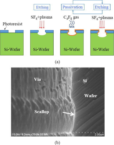
Fig. 1(a)ļŖö DRIE Ļ│ĄņĀĢ ņ¦äĒ¢ēņØś Ļ░£ļץļÅäļź╝ ļéśĒāĆļéĖ Ļ▓āņØ┤Ļ│Ā, Fig. 1(b)ļŖö ņŗżņĀ£ļĪ£ ņĀ£ņĪ░ļÉ£ ļ╣äņĢä ļ▓Įļ®┤ņØä ļ│┤ņØĖ Ļ▓āņØ┤ļŗż18). ļ╣äņĢä ļ▓Įļ®┤ņØĆ ņłśņ¦üĒÖĆņØś ĒśĢņāüņØä ļéśĒāĆļé┤ņ¦Ćļ¦ī, ņŚÉņ╣Ł ļ░Å ļ│┤ĒśĖļ¦ē ņĖĄ ļ░śļ│Ą ĒśĢņä▒Ļ│╝ņĀĢņŚÉņä£, Si ļ▓Įļ®┤ņØä ļ»ĖņäĖĒĢśĻ▓ī ļ│┤ļ®┤ ļČĆņ▒äĻ╝┤(scallop) ĒśĢņāüņØä ļéśĒāĆļéĖļŗż.
Fig.┬Ā1
Schematics of TSV drilling by DRIE process (a), and magnified via wall fabricated by DRIE (b)18)
DRIEņŚÉ ņØśĒĢ┤ ņĀ£ņĪ░ļÉśļŖö TSV ĒśĢņāüņŚÉļŖö Fig. 2ņŚÉ ļ│┤ņØĖ Ļ▓āņ▓śļ¤╝ ņłśņ¦üĒśĢ ņŖżĒŖĖļĀłņØ┤ĒŖĖ(straight) TSV(Fig. 2 (b, c)), Ļ▓Įņé¼ĒśĢ(tapered) TSV(Fig. 2(a)), ĒĢŁņĢäļ”¼ ĒśĢ ļō▒ļ░®ņä▒(isotropic) TSV(Fig. 2(d)) ļō▒ņØ┤ ņ׳ļŗż. ņØ╝ļ░śņĀüņ£╝ļĪ£ ņłśņ¦üĒśĢ TSVĻ░Ć ļ¦ÄņØ┤ ņé¼ņÜ®ļÉśļŖöļŹ░, ļÅäĻĖłņĢĪņØ┤ļéś ļÅäĻĖł ņĪ░Ļ▒┤ņØ┤ ņל ņĪ░ņĀłļÉśņ¢┤ņĢ╝ Ļ▓░ĒĢ© ņŚåļŖö CuņØś ņČ®ņĀäņØ┤ Ļ░ĆļŖźĒĢśļŗż. ĻĘĖļĀćņ¦Ć ņĢŖņ£╝ļ®┤ ņĀäļźś ļ░ĆļÅäĻ░Ć ļåÆņØĆ ņ×ģĻĄ¼ ļ¬©ņä£ļ”¼ ļČĆļČäņØś ļÅÖ ļÅäĻĖłņĖĄņØ┤ ņä£ļĪ£ ņŚ░Ļ▓░ļÉśņ¢┤ ļé┤ļČĆņŚÉ ņŗ£ņ×ä(seam) Ļ▓░ĒĢ©ņØ┤ ņāØņä▒ļÉśĻĖ░ ņēĮļŗż. ņØ┤ļź╝ Ļ░£ņäĀĒĢśĻĖ░ ņ£äĒĢ┤ ļ¬©ņä£ļ”¼ ļČĆļČäņØś ņĀäļźś ļ░ĆļÅäļź╝ ļé«ņČöĻĖ░ ņ£äĒĢ┤ ļ¬©ņä£ļ”¼ ļČĆļČäņØä ļ¬©ļö░ĻĖ░(rounding) ĒĢśĻĖ░ļÅä ĒĢ£ļŗż(Fig. 2(b)). Ļ▓Įņé¼ĒśĢ TSVļŖö ņ×ģĻĄ¼ņØś ņ¦üĻ▓ĮņØ┤ ļäōĻ│Ā ļ░öļŗźņØś ņ¦üĻ▓ĮņØ┤ ņóüņØĆļŹ░, ļŗżņ¢æĒĢ£ Ļ▓Įņé¼Ļ░üņØä ļ¦īļōż ņłś ņ׳ņ£╝ļ®░, Ļ▓Įņé¼ĒśĢ TSVĻ░Ć ņłśņ¦üĒśĢ TSVļéś ĒĢŁņĢäļ”¼ĒśĢ TSVņŚÉ ļ╣äĒĢ┤, ļÅäĻĖłņŗ£ TSV ņ×ģĻĄ¼Ļ░Ć ļ¦ēĒ׳ļŖö ĒśäņāüņØ┤ ļŹ£ ĒĢśĻĖ░ ļĢīļ¼ĖņŚÉ TSV ļé┤ ļÅäĻĖł ņČ®ņĀäņØ┤ ņÜ®ņØ┤ĒĢśļŗż. ņĀĆņ×É ļō▒ņØĆ TSV ņ×ģĻĄ¼ ņ¦üĻ▓Į 44.3 ŃÄø, ļ░öļŗź ņ¦üĻ▓Į 34.2 ŃÄø, Ļ╣ŖņØ┤ 60 ŃÄø, Ļ▓Įņé¼Ļ░üļÅä 11╦ÜņØś Ļ▓Įņé¼ĒśĢ TSVļź╝ ņĀ£ņ×æĒĢśņŚ¼ ņÜ®ņØ┤ĒĢśĻ▓ī Cu ņČ®ņĀäņØä ņŗżņŗ£ĒĢ£ ļ░ö ņ׳ļŗż19). ļ░śļ®┤ ĒĢŁņĢäļ”¼ĒśĢņØĆ TSV ņ×ģĻĄ¼ ļ¦ēĒלņŚÉ ņØśĒĢ┤ ļé┤ļČĆņŚÉ ĻĖ░Ļ│Ą(void)ņØ┤ļéś ņŗ¼(seam) Ļ▓░ĒĢ©ņØś ļ░£ņāØņØ┤ ņÜ®ņØ┤ĒĢśļŗż.

3. TSV ļé┤ļ▓ĮņØś ĻĖ░ļŖźņä▒ ļ░Ģļ¦ē ņĮöĒīģ
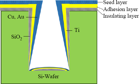
ĻĖ░ļŖźņä▒ ļ░Ģļ¦ē(functional layer)ņØĆ TSV ļé┤ļČĆņÖĆ TSVĻ░Ć ĒśĢņä▒ļÉśņ¦Ć ņĢŖņØĆ ņŗżļ”¼ņĮś ņø©ņØ┤ĒŹ╝ņŚÉ ņĀłņŚ░ņĖĄ, ņĀæĒĢ®ņĖĄ, ņŗ£ļō£ņĖĄ ļō▒ņØä ņĮöĒīģĒĢ£ļŗż. ņĮöĒīģ ļ¼╝ņ¦ł ļ░Å ņĮöĒīģ ļ¬®ņĀüņØĆ ŌæĀ ņĀłņŚ░ņĖĄ(insulating layer)ņ£╝ļĪ£ņä£, ļ│┤ĒåĄ SiO2, Ēś╣ņØĆ SiNņØä TSVņÖĆ ņŗżļ”¼ņĮś ņø©ņØ┤ĒŹ╝ņØś ņĀäĻĖ░ņĀü ņĀłņŚ░ņØä ņ£äĒĢ┤ ņĮöĒīģĒĢśĻ│Ā, ŌæĪ ņĀæĒĢ®ņĖĄ(adhesion layer)ņ£╝ļĪ£ņä£ Ti ļō▒ņØä TSV ļé┤ļČĆņØś ņČ®ņĀä ĻĖłņåŹ(ļ│┤ĒåĄ Cu)Ļ│╝ ņŗżļ”¼ņĮś ņø©ņØ┤ĒŹ╝ ņé¼ņØ┤ņØś ņĀæĒĢ®ļĀźņØä Ē¢źņāüņŗ£ĒéżĻĖ░ ņ£äĒĢ┤ ņĮöĒīģĒĢśļ®░, Ōæó ņŗ£ļō£ņĖĄ(seed layer)ņ£╝ļĪ£ņä£ Cuļéś Auļź╝, ņČ®ņĀä ĻĖłņåŹ(ļ│┤ĒåĄ Cu)ņØś ņĀäĒĢ┤ļÅäĻĖłņØä ņÜ®ņØ┤ĒĢśĻ▓ī ĒĢśĻĖ░ ņ£äĒĢ£ ņĀäņ▓śļ”¼ļĪ£ ņĮöĒīģĒĢ£ļŗż.
ĻĖ░ļŖźļ░Ģļ¦ēņĖĄņØś ņĮöĒīģ ņśłļŖö ļ¦ÄņØĆ ņäĀĒ¢ē ņŚ░ĻĄ¼ņŚÉņä£ SiO2/ Ti/Cu20)ņÖĆ Ļ░ÖņØĆ ņé¼ļĪĆĻ░Ć ļ│┤Ļ│ĀļÉśņ¢┤ ņ׳ļŗż. ņĀłņŚ░ņĖĄņ£╝ļĪ£ ĒśĢņä▒ļÉśļŖö SiO2ņØś Ļ▓ĮņÜ░ ņŗżļĀłņØĖ(SiH4)ņØä ņØ┤ņÜ®ĒĢśņŚ¼ CVDļĪ£ ņ”Øņ░®ĒĢĀ ņłś ņ׳ļŖöļŹ░, SiO2 CVD ņ”Øņ░® ņŗ£ņØś ĒÖöĒĢÖļ░śņØæņŗØņØĆ ļŗżņØīĻ│╝ Ļ░Öļŗż.
ņĀæĒĢ®ņĖĄņØĖ TiļŖö SiO2 ļō▒ņØś ņĀłņŚ░ņĖĄĻ│╝ Cu ņČ®ņĀä ĻĖłņåŹ ņ¢æņ¬ĮĻ│╝ ņĀæĒĢ®ņä▒ņØ┤ ļ¬©ļæÉ ņóŗĻĖ░ ļĢīļ¼ĖņŚÉ TSV ļé┤ļ▓ĮĒæ£ļ®┤ņØś SiO2 ņĖĄ ņ£äņŚÉ ļ░Ģļ¦ēņ£╝ļĪ£ ĒśĢņä▒ĒĢ£ļŗż. ļ¦łņ¦Ćļ¦ēņ£╝ļĪ£ ņŗ£ļō£ņĖĄņØĆ ņĀäņłĀĒĢ£ ļ░öņÖĆ Ļ░ÖņØ┤ ņČ®ņĀä ĻĖłņåŹņØĖ CuņØś ņĀäĒĢ┤ļÅäĻĖłņØä ņÜ®ņØ┤ĒĢśĻĖ░ ņ£äĒĢ┤ ņĮöĒīģĒĢśļŖöļŹ░, ņŻ╝ļĪ£ ļÅÖņóģņØś Cu ļ░Ģļ¦ēņØä ņĮöĒīģĒĢśņ¦Ćļ¦ī20) Auļź╝ ņĮöĒīģĒĢ£ ņé¼ļĪĆļÅä ņ׳ļŗż.(Fig. 3)21) ņĀĆņ×É ļō▒ņØĆ SiO2, Ti, Au ņĖĄņØä Si ļ▓Į ļé┤ņĖĪņ£╝ļĪ£ļČĆĒä░ TSV ņ¬Įņ£╝ļĪ£ ņ░©ļĪĆļīĆļĪ£ ņĮöĒīģĒĢśņśĆļŗż21-23).
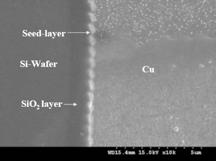
Au ņĖĄņØä ņé¼ņÜ®ĒĢśļŖö ņØ┤ņ£ĀļŖö ņé░ĒÖöļ░®ņ¦Ć ļ░Å ļÅäĻĖłņĢĪ ļé┤ņŚÉņä£ņØś ĒÖöĒĢÖņĀü ņĢłņĀĢņä▒ņØä Ļ│ĀļĀżĒĢ£ Ļ▓ĮņÜ░, AuņØś ĒŖ╣ņä▒ņØ┤ CuņŚÉ ļ╣äĒĢ┤ ņÜ░ņłśĒĢśĻĖ░ ļĢīļ¼ĖņØ┤ļŗż. Ti/Cu ļśÉļŖö Ti/AuņÖĆ Ļ░ÖņØĆ ĻĖłņåŹļ░Ģļ¦ē ĒśĢņä▒ņØĆ ņŖżĒŹ╝Ēä░ļ¦ü(sputtering)ņØä ņØ┤ņÜ®ĒĢśņŚ¼ ĒśĢņä▒ļÉśļŖö Ļ▓āņØ┤ ļ│┤ĒåĄņØ┤ļŗż. ņĀĆņ×É ļō▒ņØĆ ņĀłņŚ░ņĖĄņ£╝ļĪ£ 1 ŃÄø ļæÉĻ╗śņØś SiO2ļź╝ Ļ│Āļ░ĆļÅä ĒöīļØ╝ņ”łļ¦ł CVD(high density plasma chemical vapor deposition, HDPCVD)ļĪ£ ņĮöĒīģĒĢśĻ│Ā, ņØ┤ņ¢┤ņä£ Tiļź╝ ņĀæņ░®ņĖĄ(adhesion layer) ļ░Å Cu ļź╝ ņŗ£ļō£ņĖĄņ£╝ļĪ£ ņŖżĒŹ╝Ēä░ ņĮöĒīģņןņ╣śļĪ£(sputter coater) ņ”Øņ░®ĒĢ£ ņśłĻ░Ć ņ׳ļŗż19). Cu ņĖĄņØĆ ņĀäĻĖ░ņĀäļÅäņä▒ļÅä ņóŗĻ│Ā AuņĖĄņŚÉ ļ╣äĒĢ┤ ņĀĆĻ░ĆņØ┤ņ¦Ćļ¦ī, ņé░ĒÖöļÉśĻĖ░ ņēĮĻ│Ā ņØ┤ĒøäņØś ļ╣äņĢäļé┤ Cu ļÅäĻĖł ņČ®ņĀäĻ│ĄņĀĢņŚÉņä£ CuņĖĄņØ┤ ļÅäĻĖłņĢĪ ņżæņ£╝ļĪ£ ņÜ®ĒĢ┤ļÉśņ¢┤ ņåīļ¬©ļÉśļŖö ļŗ©ņĀÉņØ┤ ņ׳ļŗż. Fig. 4ļŖö ĻĖ░ļŖźļ░Ģļ¦ēņØ┤ TSV ļé┤ņŚÉ ĒśĢņä▒ļÉ£ ĻĄ¼ņĪ░ļź╝ ļéśĒāĆļéĖ Ļ▓āņØ┤ļŗż.
TSV ļé┤ļ®┤ņŚÉ ĒśĢņä▒ļÉśļŖö ņŗ£ļō£ņĖĄņØĆ Fig. 4 ļ│┤ļō»ņØ┤ ļ╣äņĢä ņ×ģĻĄ¼ ļČĆļČäņØ┤ ļæÉĻ╗ŹĻ│Ā ļ░öļŗź ļČĆļČäņØ┤ ņ¢ćĻ▓ī ĒśĢņä▒ļÉ£ļŗż. ņØ┤ļ¤¼ĒĢ£ ĒśäņāüņØĆ ņŗ£ļō£ņĖĄ ĻĖłņåŹņØś ņŖżĒŹ╝Ēä░ļ¦ü ņŗ£ ĻĖłņåŹ ņøÉņ×ÉĻ░Ć ļČłĻĘ£ņ╣ÖĒĢ£ ļ░®Ē¢źņ£╝ļĪ£ ņ¦üņäĀņāüņ£╝ļĪ£ ļéśņĢäĻ░ĆĻĖ░ ļĢīļ¼ĖņŚÉ ļ╣äņĢä ĒÖĆ ņ×ģĻĄ¼ ļČĆļČäņØĆ ļ░öļŗźļČĆļČäļ│┤ļŗż ĻĖłņåŹ ņøÉņ×ÉĻ░Ć ņ”Øņ░®ļÉĀ ĒÖĢļźĀņØ┤ ļŹö Ēü¼ļ®░, ņØ┤ļĪ£ ņØĖĒĢ┤ ļŹö ļæÉĻ║╝ņÜ┤ ņŗ£ļō£ ņĖĄņØ┤ ĒśĢņä▒ļÉ£ļŗż. ĻĘĖ Ļ▓░Ļ│╝ļŖö Hong ļō▒21) ņØś ņŚ░ĻĄ¼ņŚÉņä£ Fig. 5ņŚÉ ļ│┤ņØĖ Ļ▓āņ▓śļ¤╝ ņŖżĒŹ╝Ēä░ļ¦üļÉ£ Ti, Au ņŗ£ļō£ņĖĄĻ│╝ ņØ┤ņØś EDS ļČäņäØņØä ĒåĄĒĢ┤ņä£ļÅä ĒÖĢņØĖļÉ£ļŗż. ĻĘĖļ”╝ņŚÉņä£ ļ│┤ļō»ņØ┤ TSV ņ×ģĻĄ¼ ļČĆļČäņŚÉņä£ļŖö Au ņŗ£ļō£ ņĖĄņØ┤ ļæÉĻ╗ŹĻ▓ī ļéśĒāĆļéśĻ│Ā, ļ░öļŗź ļČĆļČäņŚÉņä£ļŖö ņ¢ćĻ▓ī Ļ┤Ćņ░░ļÉ£ļŗż.

4. TSV ņØś Cu ņČ®ņĀä ļÅäĻĖł
TSV ļé┤ļ▓ĮņØä ĻĖ░ļŖźņä▒ ļ░Ģļ¦ēņ£╝ļĪ£ ņĮöĒīģĒĢ£ ĒøäņŚÉ ņĀäļÅäņä▒ ĻĖłņåŹņØä TSVņŚÉ ņČ®ņĀäĒĢ£ļŗż. ļ│┤ĒåĄņØĆ ņĀäĒĢ┤ļÅäĻĖłļ▓Ģņ£╝ļĪ£ ņČ®ņĀäĒĢśņ¦Ćļ¦ī, ļ░öņĢä ĒÖĆ ņ¦üĻ▓ĮņØ┤ 1 ŃÄø ņØ┤ĒĢśļĪ£ ņĢäņŻ╝ ņ×æņØĆ Ļ▓ĮņÜ░ļéś ĒŖĖļĀīņ╣ś(trench) ņČ®ņĀäņØś Ļ▓ĮņÜ░ņŚÉļŖö ļ¼┤ņĀäĒĢ┤ļÅäĻĖłņØ┤ ņé¼ņÜ®ļÉśĻĖ░ļÅä ĒĢ£ļŗż. ņŖĄņŗØ ņĮöĒīģļ▓Ģņ£╝ļĪ£ ņØ╝ļ░śĒÖö ļÉśņ¢┤ ņ׳ļŖö ņĀäĻĖ░ļÅäĻĖłļ▓ĢņØĆ ņĀäļźśļź╝ ĒØśļĀżņä£ ņØīĻĘ╣ņØĖ Si ņø©ņØ┤ĒŹ╝ņØś ļ╣äņĢä ĒÖĆņŚÉ ĻĖłņåŹņØä ļÅäĻĖłĒĢśļŖö ļ░®ļ▓ĢņØ┤ļŗż. ņĀäĒĢ┤ ļÅäĻĖłņŗ£ ĻĖłņåŹņØĆ ļÅäĻĖłņÜ®ņĢĪņāüņØś ĻĖłņåŹņØ┤ņś©(ņśł, Cu++)ņØ┤ ņØīĻĘ╣ņŚÉņä£ ņĀäņ×Éļź╝ ļ░øņĢä ļ╣äņĢä ĒÖĆ ļé┤ļ▓ĮņØś ĻĖ░ļŖźņä▒ ĻĖłņåŹņĖĄņŚÉ ņäØņČ£ļÉ£ļŗż.
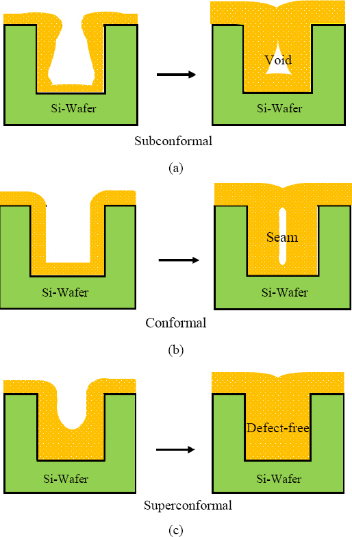
ņØīĻĘ╣ņŚÉņä£ ĒÖśņøÉ ņäØņČ£ļÉśļŖö ĻĖłņåŹņØ┤ņś©ņØś ļ¼┤Ļ▓ī(W)ļŖö ļÅäĻĖł ņĀäļźśņØś ņ¢æņŚÉ ļ╣äļĪĆĒĢśļ®░, FaradayņØś ļ▓Ģņ╣ÖņŚÉ ņØśĒĢśņŚ¼ Ļ│äņé░ļÉĀ ņłś ņ׳ļŗż(Eq. 7).
ļŗ©, Q ; ĒåĄņĀäļ¤ēņØ┤ļ®░, i ; ļÅäĻĖł ņĀäļźś(A), t ; ļÅäĻĖł ņŗ£Ļ░ä(s), Z ; ņĀäĻĖ░ĒÖöĒĢÖļŗ╣ļ¤ē(electrochemical equivalent) (g/ Coloumb), F ; Faraday ņāüņłś(96500 C/equivalent), n ; Ļ░Ćņłś
ņĀäĻĖ░ ļÅäĻĖłļ▓ĢņŚÉ ņØśĒĢ£ TSV ļé┤ CuņØś ņČ®ņĀä ļ░®ļ▓ĢņØĆ Ļ│ĄņĀĢ ļ╣äņÜ®ņØ┤ ļ╣äĻĄÉņĀü ņĀĆļĀ┤ĒĢ£ ņןņĀÉņØ┤ ņ׳ņ£╝ļ®░, ļÅäĻĖł ņĀäļźś ĒīīĒśĢņØś ņĪ░ņĀłņØ┤ļéś ņ▓©Ļ░ĆņĀ£ļź╝ Ļ░ĆĒĢ£ ļÅäĻĖłņĢĪņØä ņé¼ņÜ®ĒĢśņŚ¼ Ļ▓░ĒĢ© ņŚåļŖö ņČ®ņĀäņØ┤ Ļ░ĆļŖźĒĢśļŗż. ļśÉ, ņŗżļ”¼ņĮś ņø©ņØ┤ĒŹ╝ ļé┤ņØś ņłś ŃÄø ņ¦üĻ▓ĮņØś ņ×æņØĆ ļ╣äņĢäņØś 100 ņĀĢļÅäņØś Ļ╣ŖņØĆ ņóģĒÜĪļ╣äļź╝ Ļ░¢ļŖö Ļ┤ĆĒåĄĒÖĆĻ╣īņ¦Ć ļÅäĻĖłņØ┤ Ļ░ĆļŖźĒĢśĻ│Ā, ņ¢æņé░ņØ┤ Ļ░ĆļŖźĒĢśļ»ĆļĪ£ TSV ņČ®ņĀäņŚÉ Ļ░Ćņן ļ¦ÄņØ┤ ņé¼ņÜ®ļÉśĻ│Ā ņ׳ļŗż. TSV ļé┤ļČĆ ļ░öļŗźļČĆĒä░ CuĻ░Ć ļÅäĻĖłļÉśļŖö ļ░®ļ▓Ģ ņżæ ņĀäļźś ĒīīĒśĢ ņĪ░ņĀłņŚÉ ņØśĒĢ£ ļ░®ļ▓ĢņØĆ ņĀĆņ×É ļō▒ ņØ┤ ļ│┤Ļ│ĀĒĢ£ ļ░ö ņ׳ļŗż24). ĻĘĖļ¤¼ļéś Cu ņĀäĻĖ░ ļÅäĻĖłņŚÉ ņØśĒĢ£ TSV ņČ®ņĀäņŗ£ ņĀäļźśļ░ĆļÅäĻ░Ć TSV ņ×ģĻĄ¼ņØś ļ¬©ņä£ļ”¼ ļČĆļČäņØ┤ ļåÆĻĖ░ ļĢīļ¼ĖņŚÉ Ļ▓░ĒĢ©ņØ┤ ļ¦ÄņØ┤ ļ░£ņāØĒĢśĻĖ░ļÅä ĒĢ£ļŗż. TSV ļé┤ņŚÉ Cuļź╝ ļÅäĻĖłĒĢĀ ļĢī ļÅäĻĖłņØ┤ ņ¦äĒ¢ēļÉśļŖö ĒśĢņāüņŚÉ ļö░ļØ╝ņä£, subconformal, conformal, superconformalņØś 3 ņóģļźśļĪ£ ĻĄ¼ļČäĒĢ£ļŗż(Fig. 6). SubconformalņØĆ TSV ņ×ģĻĄ¼ļČĆļČäņŚÉņä£ ļ╣ĀļźĖ ļÅäĻĖłņØ┤ ņØ╝ņ¢┤ļéśļ®░, TSV ļé┤ļČĆĻ░Ć Cu ļÅäĻĖłļÉśĻĖ░ņĀäņŚÉ ņ×ģĻĄ¼ ļÅäĻĖłņĖĄņØ┤ ņŚ░Ļ▓░ļÉśņ¢┤ ļé┤ļČĆņŚÉ ĻĖ░Ļ│Ą(void)Ļ▓░ĒĢ©ņØ┤ ņāØņä▒ļÉ£ļŗż. ConformalņØĆ TSV ņĀäņ▓┤ņĀüņ£╝ļĪ£ ĻĘĀņØ╝ĒĢ£ ņåŹļÅäļĪ£ ļÅäĻĖłņØ┤ ņ¦äĒ¢ēļÉśļ®░, TSV ļé┤ļČĆņŚÉ ņŗ£ņ×ä Ļ▓░ĒĢ©ņØä ļé©ĻĖ┤ļŗż. Superconformal ļÅäĻĖłņØĆ TSV ļé┤ļČĆ ļ░öļŗźņŚÉņä£ ļ╣ĀļźĖ ļÅäĻĖłņØ┤ ņØ╝ņ¢┤ļéśļŖö bottom-up ņČ®ņĀäņ£╝ļĪ£ TSV ļé┤ņŚÉ Ļ▓░ĒĢ©ņØ┤ ņŚåļŖö ļÅäĻĖłļČĆļź╝ ņ¢╗ņØä ņłś ņ׳ļŗż. Ļ░ĆņåŹņĀ£ņØś ļåŹļÅäņŚÉ ļö░ļźĖ TSV ļ░öļŗźņ£╝ļĪ£ļČĆĒä░ņØś(bottom-up) Cu ņČ®ņĀäņŚÉ ļīĆĒĢśņŚ¼ Hoffmann ļō▒ņØ┤ ņŚ░ĻĄ¼ ļ│┤Ļ│ĀĒĢ£ ļ░ö ņ׳ļŗż25).
TSVņŚÉ Cuļō▒ ļÅäņĀäņä▒ ĻĖłņåŹņØä ņČ®ņĀäĒĢĀ Ļ▓ĮņÜ░, DC(direct current) ņĀäĻĖ░ļÅäĻĖłņØä ņØ┤ņÜ®ĒĢśļ®┤, ļ╣äņĢä ĒÖĆ ņ×ģĻĄ¼ņØś ļ¬©ņä£ļ”¼ ļČĆļČäņŚÉ ņĀäļźś ļ░ĆļÅäĻ░Ć ļåÆņĢäņĀĖņä£ ļ╣äņĢä ņ×ģĻĄ¼ļČĆņŚÉņä£ ņĀäņ░®ņåŹļÅäĻ░Ć ļ╣äņĢä ļ░öļŗźļ│┤ļŗż ļ╣©ļØ╝ņ¦ĆļŖö sub-conformal ļÅäĻĖłņØ┤ ļ░£ņāØĒĢśĻĖ░ ņē¼ņøīņ¦äļŗż. ļö░ļØ╝ņä£ sub-conformal ņĀäņ░®ņØä ļ░®ņ¦ĆĒĢśĻ│Ā ļ│┤ņØ┤ļō£ņÖĆ ņŗ£ņ×ä ļō▒ Ļ▓░ĒĢ©ņØ┤ ņŚåļŖö ņČ®ņĀäņØä ņ£äĒĢ┤ņä£ļŖö TSV ņ×ģĻĄ¼ļČĆņŚÉ ņĀäļźśļ░ĆļÅäņØś ņ¦æņżæņØä ļ░®ņ¦ĆĒĢ┤ņĢ╝ ĒĢ£ļŗż. ņØ┤ļź╝ ņ£äĒĢ┤ ĒÄäņŖż ņĀäļźśļź╝ ņØ┤ņÜ®ĒĢ£ ņČ®ņĀäļÅäĻĖłņØ┤ ņØ╝ļ░śņĀüņ£╝ļĪ£ ņé¼ņÜ®ļÉśĻ│Ā ņ׳ļŗż. ĻĘĖļ¤¼ļéś, Lee ļō▒26)ņØś ļ│┤Ļ│ĀņŚÉ ņØśĒĢśļ®┤, ĒÄäņŖż ņĀäļźśņØĖ PPR(periodic pulse reverse) ĒīīĒśĢņŚÉņä£ļÅä ĒÖśņøÉņĀäļźśļ░ĆļÅäļź╝ -7~-10 mA/cm2 ļĪ£ ĒĢśĻ│Ā, ņé░ĒÖöņĀäļźśļ░ĆļÅäļŖö 30~50 mA/cm2 ļ▓öņ£äņŚÉņä£ Ļ░ĆĒĢśļ®░, ņ¢æĻĘ╣ ļ░Å ņØīĻĘ╣ ņĀäĻĘ╣ ņé¼ņØ┤ņØś Ļ▒░ļ”¼ļź╝ 3 cm ĒĢśņśĆņØä ļĢī, ļÅäĻĖł ņ┤łĻĖ░ņŚÉ ļ╣äņĢä ļ░öļŗźļČĆĻ░Ć ļ»Ėņ▓ś ļÅäĻĖłļÉśĻĖ░ ņĀäņŚÉ TSVņØś ņ×ģĻĄ¼ļČĆĻ░Ć ļ¦ēĒ׳Ļ▓ī ļÉśļŖö sub-conformal ņĀäņ░®ņØ┤ ļéśĒāĆļé¼ļŗż. ņØ┤ļĪ£ ņØĖĒĢśņŚ¼, TSV ļé┤ļČĆņŚÉ ļ│┤ņØ┤ļō£ņÖĆ ņŗ£ņ×ä ļō▒ņØś Ļ▓░ĒĢ©ņØ┤ ļ░£ņāØĒĢśĻ▓ī ļÉ£ļŗż(Fig. 7(a)).
Fig.┬Ā7
Void creation by over-growth of electro-deposited Cu at the top point (a),26) and middle point of via (b)27)

ļĢīļĪ£ļŖö ļ╣äņĢäņØś ņżæĻ░äļČĆļČäņŚÉņä£ ļ©╝ņĀĆ ļÅäĻĖłņØ┤ ņØ╝ņ¢┤ļéśņä£ ņØ┤ļōż ļÅäĻĖłļČĆĻ░Ć ņŚ░Ļ▓░ļÉśļ®┤ņä£, ļ╣äņĢä ļ░öļŗźņ¬ĮņŚÉ voidņÖĆ seam ļō▒ņØś Ļ▓░ĒĢ©ņØ┤ ļ░£ņāØļÉśļŖö ļÅäĻĖłņØ┤ ļéśĒāĆļéśĻĖ░ļÅä ĒĢ£ļŗż Hong ļō▒27)ņŚÉ ņØśĒĢśļ®┤, ĒÅēĻĘĀ ņĀäļźś ļ░ĆļÅä -7.71 mA/cm2ņØś PPR ņĀäļźś ĒīīĒśĢņØä ņØ┤ņÜ®ĒĢ£ Cu ņČ®ņĀäņŚÉņä£ ņ¢æĻĘ╣ ļ░Å ņØīĻĘ╣ ņĀäĻĘ╣ ņé¼ņØ┤ņØś Ļ▒░ļ”¼ļź╝ 3 cm ĒĢśņśĆņØä ļĢī, Fig. 7(b)ņÖĆ Ļ░ÖņØĆ Cu ņČ®ņĀä ĒśĢņāüņØ┤ ļéśĒāĆļé£ļŗż. ņØ┤Ļ▓āņØĆ ĒÄäņŖż ņĀäļźśļź╝ ņé¼ņÜ®ĒĢśļŹöļØ╝ļÅä TSV ļ░öļŗźļČĆĒä░ ņÜ░ņäĀ ļÅäĻĖłļÉśļŖö bottom-up ļÅäĻĖłņØ┤ ļČĆņĪ▒ĒĢśņŚ¼, TSV ņ¢æņ¬Į ļ▓ĮņŚÉņä£ ņä▒ņןĒĢ┤ ļéśņś© ĻĄ¼ļ”¼ ņĖĄņØ┤ TSV ņżæņŗ¼ļČĆņŚÉņä£ ļ¦īļéś and middle point of via (b)27).
ļÅäĻĖłņ×æņŚģņŚÉņä£ ĒÄäņŖż ņĀäļźśļŖö ņØīĻĘ╣ņŚÉ ļÅäĻĖłņØä ņØ╝ņ£╝ĒéżļŖö ĒÖśņøÉņĀäļźśņÖĆ Ļ│╝ļÅäĻĖłņĖĄņØä ļŗżņŗ£ ņÜ®ĒĢ┤ņŗ£ĒéżļŖö ņé░ĒÖöņĀäļźśļź╝ ļ▓łĻ░łņĢä Ļ░ĆĒĢ£ļŗż. ņØ┤ļź╝ ĒåĄĒĢśņŚ¼, ĒÖśņøÉņĀäļźśļ¦ī ĒØÉļź╝ ļĢīņØś TSV ņ×ģĻĄ¼ ļ¬©ņä£ļ”¼ļČĆņØś ņĀäļźś ņ¦æņżæĒÜ©Ļ│╝ļź╝ ņÖäĒÖöĒĢśņŚ¼, ļ╣äņĢä ņ×ģĻĄ¼ļČĆņŚÉņä£ ļÅäĻĖłņåŹļÅäļź╝ ņĀĆĻ░Éņŗ£ņ╝£ ļ╣äņĢä ĒÖĆņØś ņ×ģĻĄ¼ļČĆĻ░Ć ļ¦ēĒ׳ļŖö ĒśäņāüņØä ņ¢ĄņĀ£ĒĢ£ļŗż. ĒÄäņŖżņĀäļźśņŚÉļŖö ņé░ĒÖöņĀäļźś ļīĆņŗĀ ļÅäĻĖłņĀäļźśļź╝ 0 ņ£╝ļĪ£ ĒĢśņŚ¼, ļÅäĻĖłņåŹļÅäļ¦īņØä 0ņ£╝ļĪ£ ĒĢśļŖö ļ░®ļ▓ĢļÅä ņ׳ņ£╝ļéś, ņé░ĒÖöņĀäļźśļź╝ Ļ░ĆĒĢśļŖö ļ░®ļ▓ĢņŚÉ ļ╣äĒĢ┤ Ļ│╝ļÅäĻĖł ņ¢ĄņĀ£ņØś ĒÜ©Ļ│╝Ļ░Ć ļ¢©ņ¢┤ņ¦äļŗż.
ĒÄäņŖżņŚÉ ņØśĒĢ£ ņĀäļźś ĒīīĒśĢ ņĪ░ņĀłņŚÉ ļŹöĒĢśņŚ¼, ļÅäĻĖłņĢĪņŚÉ ļÅäĻĖłņåŹļÅä ņ¢ĄņĀ£ņĀ£ ļ░Å Ļ░ĆņåŹņĀ£ļź╝ ņ▓©Ļ░ĆĒĢśņŚ¼ Ļ▓░ĒĢ©ļ░£ņāØņØä ņ¢ĄņĀ£ĒĢśļ®┤ņä£ ļ╣ĀļźĖ ļÅäĻĖłņØä ĒĢśĻĖ░ļÅä ĒĢ£ļŗż(Fig. 8 ņ░ĖņĪ░). ņ¢ĄņĀ£ņĀ£ļĪ£ļŖö ĒØöĒ׳ polyethylene glycol(PEG)ļź╝ ņé¼ņÜ®ĒĢśĻ│Ā19,28), Ļ░ĆņåŹņĀ£ļĪ£ļŖö bis-(3-sodiumsulfopropyl) disulfide(SPS) ļō▒ņØ┤ ņé¼ņÜ®ļÉ£ļŗż29).
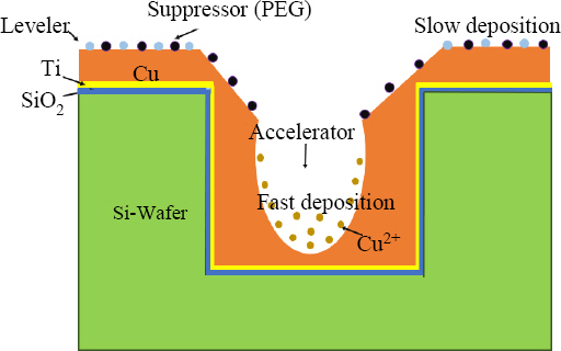
TSV ļé┤ņŚÉ Ļ▓░ĒĢ© ņŚåļŖö Cu ļÅäĻĖł ņČ®ņĀäĻ│╝ Ļ┤ĆļĀ©ĒĢśņŚ¼, Hong ļō▒21) ņŚÉ ņØśĒĢśļ®┤ TSV ļé┤ Cu ņČ®ņĀäņŗ£ ņĀĢ(+)ĒÄäņŖż ņĀäļźśļ░ĆļÅäļź╝ 1000 mA/dm2 ļĪ£ 5 ņ┤łĻ░ä ņØĖĻ░ĆĒĢśĻ│Ā, ņŚŁ(-)ĒÄäņŖż ņĀäļźśļ░ĆļÅäļź╝ 190 mA/dm2ļĪ£ 25 ņ┤łĻ░ä ņØĖĻ░ĆĒĢśņŚ¼ ņ┤Ø 57.6 ks ļÅÖņĢł ļÅäĻĖłĒ¢łņØä ļĢī Ļ▓░ĒĢ©ņØ┤ ņŚåļŖö ņÖäņĀäĒĢ£ Cu ņČ®ņĀäņØä ĒĢĀ ņłś ņ׳ņŚłļŗż(Fig. 9).
Fig.┬Ā9
Void-free electro-deposition of Cu in TSV(Cu filling in TSV in conditions of the forward pulse of 1000 mA/dm2 for 5s and reverse pulse of 190 mA/dm2 for 25 s)21)

Fig. 10ņØĆ TSV ļé┤ņŚÉ CuņØś ļ╣ĀļźĖ ļÅäĻĖł ņČ®ņĀäņØä ņ£äĒĢśņŚ¼, ĒÖśņøÉ ņĀäļźśņÖĆ ņé░ĒÖö ņĀäļźśļź╝ Ļ░ĆĒĢ£ Ēøä ņ¦¦ņØĆ ņŗ£Ļ░ä ļÅÖņĢł ņĀäļźśļź╝ ņØĖĻ░ĆĒĢśņ¦Ć ņĢŖļŖö Ē£┤ņ¦ĆĻĖ░Ļ░ä(current-off duration)ņØä ļæÉļŖö ĒÄäņŖż-ņŚŁĒÄäņŖż ņĀäļźś(PPR) ĒīīĒśĢņØä ņØ┤ņÜ®ĒĢ£ Ļ│ĀņåŹ ņĀäĒĢ┤ ļÅäĻĖłļ▓ĢņØś ļÅäĻĖłĻĖ░ĻĄ¼(plating mechanism)ļź╝ ļ│┤ņØĖ Ļ▓āņØ┤ļŗż.

ĒÄäņŖż-ņŚŁĒÄäņŖż ņĀäļźśļź╝ ņé¼ņÜ® ĒĢĀ Ļ▓ĮņÜ░, ĒÖśņøÉ ņĀäļźś ĻĖ░Ļ░äņŚÉ TSV ļé┤ņŚÉ CuĻ░Ć ļÅäĻĖłļÉśĻ│Ā, ņé░ĒÖö ņĀäļźśļ░ĆļÅäĻ░Ć Ļ▒Ėļ”¼ļŖö ņŚŁĒÄäņŖż ĻĖ░Ļ░äņŚÉ TSV ņ×ģĻĄ¼ ļ¬©ņä£ļ”¼ ļō▒ Ļ│╝ļÅäĻĖłļÉ£ ļČĆļČäņØś Cu ņĖĄņØ┤ ļÅäĻĖłņĢĪ ņżæņ£╝ļĪ£ ļŗżņŗ£ ņÜ®ĒĢ┤ļÉ£ļŗż. ņĀäļźśĻ░Ć Ļ║╝ņ¦ĆļŖö Ē£┤ņ¦ĆĻĖ░Ļ░äņŚÉļŖö TSV ņŻ╝ņ£äņØś ņÜ®ĒĢ┤ļÉ£ Cu ņØ┤ņś©ņØ┤ ļÅäĻĖłņĢĪ ņåŹņ£╝ļĪ£ ļåŹļÅäņ░©ņŚÉ ņØśĒĢ┤ ĒÖĢņé░ĒĢ┤ ĒŹ╝ņĀĖļéśĻ░äļŗż. ņØ┤ļ¤░ Ļ│╝ņĀĢņ£╝ļĪ£ ņØĖĒĢśņŚ¼, TSV ņ×ģĻĄ¼ļŖö ļ¦ēĒ׳ņ¦Ć ņĢŖĻ│Ā Ļ░£ļ░®ļÉ£ ņāüĒā£ļź╝ ņ£Āņ¦ĆĒĢśļ®░, TSV ļé┤ļČĆņŚÉ ļ│┤ņØ┤ļō£ņÖĆ ņŗ£ņ×ä ļō▒ņØś Ļ▓░ĒĢ©ņØ┤ ņ¢ĄņĀ£ļÉ£ļŗż.
TSV ļé┤ņŚÉ Cu ņČ®ņĀäņŗ£ ĒÄäņŖż ņĀäļźśļź╝ ņé¼ņÜ®ĒĢśļ®┤, ļÅäĻĖłĻ│╝ ņŚÉņ╣ŁņØ┤ ļ░śļ│ĄļÉśĻĖ░ ļĢīļ¼ĖņŚÉ TSV ļé┤ Cu ņČ®ņĀä ņŗ£Ļ░äņØ┤ ĻĖĖņ¢┤ņ¦ĆļŖö ļŗ©ņĀÉņØ┤ ņ׳ļŗż. ļö░ļØ╝ņä£ TSVņØś ņČ®ņĀä ņŗ£Ļ░äņØä ļŗ©ņČĢĒĢśĻ│Āņ×É ĒĢśļŖö ņŚ░ĻĄ¼Ļ░Ć ņ¦äĒ¢ēļÉśĻ│Ā ņ׳ļŗż. Hong ļō▒30) ņØĆ TSV ļé┤ ļÅäĻĖłņåŹļÅä Ē¢źņāüņØä ņ£äĒĢ┤ Cu ĒĢ®ĻĖłņØä ņé¼ņÜ®ĒĢ£ TSV ņČ®ņĀäņØä ļ│┤Ļ│ĀĒĢśņśĆļŗż. Cu-Ni ĒĢ®ĻĖł ļÅäĻĖłņØä ņØ┤ņÜ®ĒĢ£ TSVņØś PPRļÅäĻĖł ņČ®ņĀäņŚÉņä£, ņł£ĻĖłņåŹ Cu ņČ®ņĀäņŚÉ ļ╣äĒĢ┤ ļÅäĻĖłņŗ£Ļ░ä 20ļČä ĻĖ░ņżĆņ£╝ļĪ£ ņĢĮ 1.36 ļ░░ ļ╣ĀļźĖ Ļ▓░ĒĢ© ņŚåļŖö Ļ│ĀņåŹ ņČ®ņĀäņØä ļŗ¼ņä▒ĒĢśņśĆļŗż. ĒĢ£ĒÄĖ, Ha ļō▒31) ņØĆ ņ¦üĻ▓Į 3 ŃÄø, Ļ╣ŖņØ┤ 27 ŃÄø ņØś TSVņŚÉ ļīĆĒĢ┤ ļÅäĻĖłņĢĪļé┤ņØś sulfonated diallyl dimethyl ammonium chloride copolymer (SDDACC) ņ▓©Ļ░ĆņĀ£ ņĄ£ņĀüĒÖöļź╝ ĒåĄĒĢ┤, ļŗ© 3ļČäļ¦īņŚÉ TSV ļé┤ņŚÉ CuņØś ņČ®ņĀäņØä ņÖäļŻīĒĢśļŖö ņ┤łĻ│ĀņåŹ Cu ņČ®ņĀä ņŚ░ĻĄ¼ Ļ▓░Ļ│╝ļź╝ ļ░£Ēæ£ĒĢśĻĖ░ļÅä ĒĢśņśĆļŗż.
ļśÉĒĢ£, TSV ļé┤ Cu ļÅäĻĖłĒøä ņ¢┤ļŗÉļ¦ü ņ▓śļ”¼ņŗ£ TSVļĪ£ļČĆĒä░ Cu ļÅäĻĖłņĖĄ ļÅīņČ£ņØĆ Si ņ×¼ņ¦łņØś TSV ļ▓ĮĻ│╝ Cu ļÅäĻĖłņĖĄ ņé¼ņØ┤ņŚÉ ņŚ┤ĒīĮņ░Į Ļ│äņłś ņ░©ņØ┤ņŚÉ ņØśĒĢ£ ņØæļĀźņØä ņ£Āļ░£ĒĢśļ®░, ņØ┤ļŖö Cu ļÅäĻĖłļÉ£ TSV Ļ│äļ®┤ņØś ĻĘĀņŚ┤ ļ░Å ņłśļ¬ģ ļŗ©ņČĢņØä ņØ╝ņ£╝Ēé©ļŗż. ņØ┤ļ¤¼ĒĢ£ ļ¼ĖņĀ£ņĀÉņØä ĒĢ┤Ļ▓░ĒĢśĻĖ░ ņ£äĒĢśņŚ¼ Cu ļÅäĻĖłņĖĄņØś ļÅīņČ£ ņ¢ĄņĀ£Ļ░Ć ĒĢäņÜöĒĢ£ļŹ░, ņØ┤ļź╝ ņ£äĒĢ┤ Cu-Ni ĒĢ®ĻĖł ļÅäĻĖłņØ┤ ļ│┤Ļ│ĀļÉśņŚłļŗż. Jung ļō▒32)ņØĆ TSV ļé┤ Cu-Ni ļÅäĻĖłņØä ĒåĄĒĢśņŚ¼, 450┬░C ņ¢┤ļŗÉļ¦ü ņĪ░Ļ▒┤ņŚÉņä£ Cu-Ni ļÅäĻĖłļČĆ(cu plug)ļŖö ņĢĮ 1250 nm ļÅīņČ£ļÉśņŚłļŖöļŹ░, ņØ┤ļŖö Ļ░ÖņØĆ ņĪ░Ļ▒┤ņŚÉņä£ņØś Cu ļÅäĻĖłļČĆ ļÅīņČ£ĻĖĖņØ┤ 1360 nm ņŚÉ ļ╣äĒĢ┤ 8.8% ļÅīņČ£ ĻĖĖņØ┤Ļ░Ć Ļ░ÉņåīļÉ£ Ļ▓āņØ┤ļŗż.
ĒĢ£ĒÄĖ, 2.5D, 3D ļō▒ņØś ņ¦æņĀü ļ░śļÅäņ▓┤ ļööļ░öņØ┤ņŖżņØś Ēī©Ēéżņ¦Ģ Ļ│╝ņĀĢņŚÉņä£, TSVņØś ĒśĢņä▒Ļ│╝ Cu ņČ®ņĀä ļÅäĻĖł ļ¼ĖņĀ£ ņØ┤ņÖĖņŚÉļÅä, Si ņø©ņØ┤ĒŹ╝ņØś ĻĖ░Ļ│äĒÖöĒĢÖņĀü ņŚ░ļ¦ł(CMP)ņŚÉ ņØśĒĢ┤ ņø©ņØ┤ĒŹ╝ņØś ļæÉĻ╗śĻ░Ć 100 ŃÄø ņØ┤ĒĢśļĪ£ ņ¢ćņĢäņ¦ÉņŚÉ ļö░ļØ╝, ņø©ņØ┤ĒŹ╝ņØś ņĘ©ĻĖēņØä ņÜ®ņØ┤ĒĢśĻ▓ī ĒĢśļŖö ņ×äņŗ£ļ│Ėļö®(temporary bonding, TB) ļ░Å ļööļ│Ėļö®(debonding) ĻĖ░ņłĀņØ┤ ļśÉĒĢ£ ņżæņÜöĒĢ┤ņ¦ĆĻ│Ā ņ׳ļŗż33-35). ļööļ│Ėļö®Ļ│╝ ļ│Ėļö® ņä▒ļŖźņØĆ ļ¬©ļæÉ ņĀæņ░®ņĀ£ņŚÉ ņØśĒĢ┤ ļ¦ÄņØ┤ ņóīņÜ░ļÉ£ļŗż. ņĀæņ░®ņĀ£ ļ░Å ņĀæņ░® Ļ│ĄņĀĢ ĻĖ░ņłĀņŚÉ ļīĆĒĢ┤ Ļ░äļץĒ׳ ņä£ņłĀĒĢśļ®┤ ļŗżņØīĻ│╝ Ļ░Öļŗż. ņ”ē, TB ņĀæņ░®ņĀ£ ņåīņ×¼ļĪ£ļŖö ņŗżļ”¼ņĮśņØ┤ļéś ĒÅ┤ļ”¼ņØ┤ļ»Ėļō£ ļō▒ņØä ņé¼ņÜ®ĒĢĀ ņłś ņ׳Ļ│Ā, Si ņø©ņØ┤ĒŹ╝ņØś ņ╝Ćļ”¼ņ¢┤ļŖö ņŗżļ”¼ņĮśņØ┤ļéś, ņ£Āļ”¼ļź╝ ņé¼ņÜ®ĒĢĀ ņłś ņ׳ņ£╝ļ®░, ļ│Ėļö® ņś©ļÅäļŖö ņŗżļ”¼ņĮś ņĀæņ░®ņĀ£ņØś Ļ▓ĮņÜ░ ņĢĮ 180┬░C ļé┤ņÖĖ, ĒÅ┤ļ”¼ņØ┤ļ»Ėļō£ ņĀæņ░®ņĀ£ņØś Ļ▓ĮņÜ░ ņĢĮ 350┬░C ņĀĢļÅäņØ┤ļŗż. ļ│Ėļö®ļČĆņØś ņŚ┤ņĀü ņĢłņĀĢņä▒ņØĆ ņŗżļ”¼ņĮś ņĀæņ░®ņĀ£ņØś Ļ▓ĮņÜ░ ņĢĮ 250┬░C, ĒÅ┤ļ”¼ņØ┤ļ»Ėļō£ ņĀæņ░®ņĀ£ņØś Ļ▓ĮņÜ░ ņĢĮ 350┬░C ņØ┤ņāüņØ┤ļŗż. ļööļ│Ėļö® ļ░®ļ▓ĢņØĆ 4Ļ░Ćņ¦Ć ņĀĢļÅäļĪ£ ļéśļłī ņłś ņ׳ļŖöļŹ░, ņŚ┤ņĀü ņŖ¼ļØ╝ņØ┤ļō£ ņśżĒöä(slide-off)ļ▓Ģ, ĒÖöĒĢÖņĀü ņÜ®ĒĢ┤ļ▓Ģ, ļĀłņØ┤ņĀĆ ļ│┤ņĪ░ļ▓Ģ(ņŚæņŗ£ļ©Ė ļĀłņØ┤ņĀĆ ļō▒ ņé¼ņÜ®), ļ”¼ĒöäĒŖĖ ņśżĒöä(lift-off)ļ▓Ģ ļō▒ņØ┤ ņ׳ļŗż36). ņØ┤ņŚÉ Ļ┤ĆĒĢ£ ļ│┤ļŗż ņāüņäĖĒĢ£ ņä£ņłĀņØĆ ņ¦Ćļ®┤ Ļ┤ĆĻ│äņāü, ņØ┤ĒøäņØś ļ”¼ļĘ░ ļģ╝ļ¼ĖņŚÉņä£ ļŗżļŻ©ĻĖ░ļĪ£ ĒĢśĻ│Ā, ļ¼ĖĒŚīņØä ņ░ĖĻ│ĀĒĢ┤ ņŻ╝ĻĖ░ ļ░öļ×Ćļŗż.
ņØ┤ņāüņŚÉņä£ ļ░śļÅäņ▓┤ Si ņ╣®ņØś 3ņ░©ņøÉ ņĀüņĖĄ ņŗżņןņØä ņ£äĒĢ£ TSV ņŚ░ĻĄ¼ļōżņŚÉ ļīĆĒĢ┤ ņé┤ĒÄ┤ ļ│┤ņĢśļŗż. ĻĖłĒøäņØś 3ņ░©ņøÉ ņŗżņןĻĖ░ņłĀņØś ļ░£ņĀäĻ│╝ Ļ┤ĆļĀ©ĒĢśņŚ¼, ņø©ņØ┤ĒŹ╝ ļĀłļ▓©ņØś 3ņ░©ņøÉ ņŗżņןņŚÉņä£ļŖö ņø©ņØ┤ĒŹ╝ Ēæ£ļ®┤ņØś Ļ▒░ņ╣ĀĻĖ░ļź╝ 1 nm ņØ┤ĒĢśļĪ£ ĒĢśļŖö ĒÖöĒĢÖĻĖ░Ļ│äņĀü ņŚ░ļ¦ł(CMP, chemical mechanical polishing), ņø©ņØ┤ĒŹ╝ ļÆĘļ®┤ņØś ņŚ░ļ¦łĻĖ░ņłĀ, ņø©ņØ┤ĒŹ╝Ļ░äņØś ņĀæĒĢ®(WoW, wafer on wafer) ļō▒1)ļÅä IoT, 5G, AI, HPC ļō▒ 3ņ░©ņøÉ ņŗżņן ņĀüņÜ®ļČäņĢ╝ņØś ņøÉĻ░Ć ņĀłĻ░ÉņØä ņ£äĒĢ┤ ļŹöņÜ▒ ņŚ░ĻĄ¼ĒĢĀ ĒĢäņÜöĻ░Ć ņ׳ļŗżĻ│Ā ĒīÉļŗ©ļÉ£ļŗż.
5. Ļ▓░ ļĪĀ
ļ│Ė Ļ│ĀņŚÉņä£ļŖö Si ņø©ņØ┤ĒŹ╝ņŚÉ TSVļź╝ ņØ┤ņÜ®ĒĢ£ 3ņ░©ņøÉ Ļ│Āļ░ĆļÅä Ēī©Ēéżņ¦ĢņŚÉ ļīĆĒĢśņŚ¼ ņŚ░ĻĄ¼ ļÅÖĒ¢źņØä ņĪ░ņé¼ ļ│┤Ļ│ĀĒĢśņśĆļŗż. AI, IoT, 5G, HPC ļō▒ ļ¦ÄņØĆ ņĄ£ņŗĀ Ēś╣ņØĆ ļ»ĖļלņØś ņĀäņ×ÉĻĖ░ĻĖ░ņÖĆ ĻĖ░ņłĀ ļČäņĢ╝ņŚÉņä£ Ļ│Āņ¦æņĀü Ļ│Āņä▒ļŖź ņĀäņ×ÉĒī©Ēéżņ¦Ģ ĻĖ░ņłĀņØ┤ ĒĢäņÜöĒĢśļ®░, 3ņ░©ņøÉ ņ¦æņĀüĻĖ░ņłĀņØĆ ņØ┤ņŚÉ ĻĖ░ņŚ¼ĒĢśļŖö ļ░öĻ░Ć ņĀÉņĀÉ ņ╗żņ¦ĆĻ│Ā ņ׳ļŗż. 3ņ░©ņøÉ ņŗżņן ĻĖ░ņłĀ ņżæ ņ¦æņĀüļÅäĻ░Ć ļåÆņØĆ Si ņø©ņØ┤ĒŹ╝ ņāüņØś TSVļŖö DRIE Ļ│ĄņĀĢņŚÉ ņØśĒĢ┤ ņłśņ¦ü ĒÖĆņØä ļ¦īļōżĻ│Ā ņŗżņן ļ░ĆļÅäļź╝ ļåÆņØ┤ĻĖ░ ņ£äĒĢ┤ ņ¦üĻ▓Į ņłś ŃÄø ņĀĢļÅäņØś TSVļź╝ ĒśĢņä▒ĒĢśĻ│Ā, ņóģĒÜĪļ╣ä 100ņØś ņĢäņŻ╝ Ļ╣ŖņØĆ ĒÖĆĻ╣īņ¦Ć ņĀ£ņĪ░ĒĢ£ļŗż. ņØ┤ļ¤¼ĒĢ£ TSVņØś Ļ│Āļ░ĆļÅäĒÖöņŚÉ ļÅÖļ░śļÉśļŖö TSV Ļ░äņØś Cu ņØ┤ļÅÖ(migration)ņŚÉ ņØśĒĢ£ ņĀłņŚ░ĒīīĻ┤┤, TSVņØś ņĀĆĒĢŁ, ņØĖļŹĢĒä┤ņŖż ļō▒ ņĀäĻĖ░ņĀü ļ¼ĖņĀ£, TSVņØś ņāüĒśĖ Ļ░äņäŁ ļ¼ĖņĀ£, Cu ļÅäĻĖłņĖĄņØś Ļ▓░ĒĢ© ņ¢ĄņĀ£ņÖĆ ļ╣Āļź┤Ļ│Ā ņĀĢĒÖĢĒĢ£ Ļ▓░ĒĢ©ņØś ĒāÉņ¦Ć, ņØæļĀźļ░£ņāØ, ņø©ņØ┤ĒŹ╝ņØś ļ│┤ļŗż ļ»ĖņäĖĒĢ£ ņŚ░ļ¦ł ļ░Å ņāØņé░ņä▒ Ē¢źņāü ļō▒ņØä ĒĢ┤Ļ▓░ĒĢśļŖöļŹ░ ļ¦ÄņØĆ ļģĖļĀźņØ┤ ĒĢäņÜöĒĢĀ Ļ▓āņ£╝ļĪ£ ĒīÉļŗ©ļÉ£ļŗż. ĻĖłĒøä Ļ░ĆņåŹĒÖöĒĢśļŖö ņĀäņ×ÉĻĖ░ĻĖ░ņÖĆ ļČĆĒÆłņØś ņä▒ļŖźļ░£ņĀäĻ│╝ Ļ▓Įļ░Ģļŗ©ņåīĒÖöņŚÉ ļīĆņØæĒĢśņŚ¼ Si ņ╣®ņØś 3ņ░©ņøÉ ņĀüņĖĄĻĖ░ņłĀņŚÉ ļīĆĒĢ£ ļŹö ļ¦ÄņØĆ ņŚ░ĻĄ¼ņÖĆ ļ░£ņĀäņØä ĻĖ░ļīĆĒĢ£ļŗż.
 PDF Links
 PubReader
 ePub Link
 Full text via DOI
 Download Citation
 Print
Print