MLCC Solder Joint Property with Vacuum and Hot Air Reflow Soldering Processes
진공 및 열풍 리플로우 솔더링 접합공정에 따른 MLCC 접합특성
Article information
Abstract
After the joining of small 1005 and 0603 multilayer ceramic capacitor (MLCC) components for a semiconductor package using Type 4 (T4) and Type 7 (T7) Sn-3.0Ag-0.5Cu (SAC305), T4 Sn-1.0Ag-0.5Cu (SAC105), and T4 Sn-0.3Ag-0.7Cu (SAC0307) solder pastes, the differences between hot air reflow and vacuum soldering processes were compared in terms of void content, shear strength, and microstructure. Results showed that the hot air reflow soldering process exhibited a stable joint with a void content of 5% or less, and the vacuum soldering condition significantly reduced the void content of the solder joint as the soldering proceeded in a vacuum state. The shear strength of the SAC305 solder joint with the same powder particle size was measured to be greater for the shear strength of the vacuum soldered joint as compared to the reflow process. The vacuum soldering process was effective in removing voids during the void joining process and contributed to an improved joint strength of the solder joint by reducing the void content. When the same soldering process was applied using the 1005 MLCC chip component, the bonding strength of the T4 SAC305 solder was slightly higher than those of the SAC105 and SAC0307 solders. However, the overall initial bonding strengths were similar. The e ffects of Ag content within 0.3-3.0 wt% on the initial bonding strengths of the solders were judged to be the same. Diverse Cu6Sn5, Ag3Sn, (Ni,Cu,Pd)3Sn4, (Cu,Ni)6Sn5, NiP, and Ni3P intermetalli ccompounds (IMCs) were formed at the interfaces between the electroless nickel/electroless palladium/immersion gold finish substrate and SAC solder joint. The IMC types were constant regardless of Ag content and solder type, and the IMCs contributed to the initial solder joint strength.
1. Introduction
High memory speed is an essential requirement for implementation of next-generation smart devices and network servers, and in order to increase the memory speed, the number of bumps in semiconductor devices needs to be increased, which leads to an exponential increase in the number of bump junctions. Furthermore, with the increase in the number of bumps, the finer pitch between bumps is required, calling for packaging technology with ultrafine bump pitch ≤100 ㎛1-5). Implementation of fine pitch joints is not achieved by a single technology but requires combination of core technologies in plating, bonding, and molding. However, contrary to the world-leading position of domestic technology in fabrication of memory semiconductors and multilayer ceramic capacitors (MLCC), the key components of electronic devices, the rate of localization in the areas of plating materials, process equipment and MLCC electrode materials used in semiconductor wiring process and MLCC fabrication is low.
In order to achieve localization in product development and commercial application, assurance in product performance and reliability in high durability is instrumental for domestic semiconductor packaging components and embedded passive components such as MLCC. With the recent increase in the use of mobile devices and variety of application programs, the use of application processor (AP) modules for concurrent processing of multiple functions has shown a sharp increase4,5). The number of I/O systems is rapidly increasing in AP modules, and passive components such as MLCC are embedded in the modules. At the same time, the overall trend is that AP modules used in mobile devices are becoming lighter, thinner, and smaller, and the size of passive components such as MLCCs embedded in the modules is also decreasing from 1005 to ultrasmall MLCC such as 0603 or 0402. For bonding of Si semiconductor devices with more than 1,000 bumps, thermal compression bonding (TC bonding) or flip chip bonding is used in which bonding is performed with the application of heat and pressure. On the other hand, in the case of ultra-small MLCC components, which are passive components, modularization is implemented through the hot air reflow soldering process, a typical soldering process. However, in the case of hot air reflow soldering process, the area of the MLCC electrode is decreasing in line with the trend of the miniaturization of parts, leading to degradation in long-term bonding durability due to void formation in the MLCC solder joints.
Therefore, in this study, using the ultra-small MLCC components of 1005 and 0603 actually mounted in the semiconductor packages and the ternary Pb-free solder paste of Sn-Ag-Cu with the powder particle sizes of Type 4 (T4) and Type 7 (T7), optimization of soldering process was performed for the small passive components with the void content of the solder joints within 3.0%. In order to minimize the void content of the solder joints, the conventional hot air reflow soldering and vacuum soldering processes were respectively applied to optimize the process for minimization of void defects in the joint.
2. Experimental method
2.1 Substrates and MLCC components for semi- conductor packaging
As shown in Fig. 1, a substrate made of bismaleimide triazine (BT), a type of thermosetting polyimide resin, was used in the experiment for the flip-chip chip- scale-package (FCCSP) substrate. The BT material is an insulator mainly containing bismaleimide and triazine resin. BT resin is a plastic material, mainly used in printed circuit boards bridging semiconductors (chips) in smartphones and PCs with its excellent heat resistance. The thickness of the BT substrate was 0.3 mm, and the surface of the pad of the BT substrate was treated with electroless nickel/ electroless palladium/ immersion-gold (ENEPIG) plating. The thickness of the surface treatment was 3-8 ㎛ for Ni, 0.05-0.15 ㎛ for Pd, and 0.05-0.15 ㎛ for Au.

Overview of flip-chip chip scale packaging, (a) schematic drawing and (b) optical micrograph of BT substrate
Fig. 2 shows an image of the MICC components mounted on the BT substrate. The 1005 MLCC components (1.00(L)×0.50(W)×0.50(t) mm, 2.2-22 ㎌) and 0603 MLCC (0.60(L)×0.30) (W) × 0.33 (t) mm, 1-4 ㎌) components manufactured by Samsung Electro-Mechanics were used (4). For the plating of terminal electrodes of MLCC components, Ni electro-underlayer-coating and Sn plating were applied. The widths of the electrodes plated on the 0603 and 1005 MLCC terminals were 0.15±0.05 mm and 0.25±0.05 mm, respectively.
2.2 Pb-free solder paste and printing process
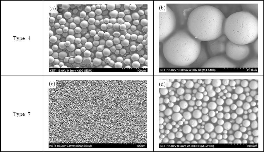
For comparison of MLCC bonding properties with different powder sizes, four types of pastes were used for the Pb-free solders in real MLCC components as shown in Table 1. The four types of solder paste used with the Pb-free solder were: T4 and T7 Sn-3.0Ag0.5Cu (SAC305), T4 Sn-1.0Ag-0.5Cu (SAC105) and T4 Sn-0.3Ag-0.7Cu (SAC0307). As shown in Fig. 3, the difference between the powder sizes of Type 4 and Type 7 solder paste can be seen in the SEM (Scanning electron microscope) micrographs. Since the powder of Type 7 solder paste is very fine from the image, it is judged to be more suitable for fine pitch solder paste printing.
The solder paste printing was performed with an area ratio aperture of 100% using a metal mask made of 100 ㎛ thick SUS material. After the printing, the printing status of the solder paste was examined using a 30x optical microscope.
2.3 Hot air reflow soldering and vacuum soldering
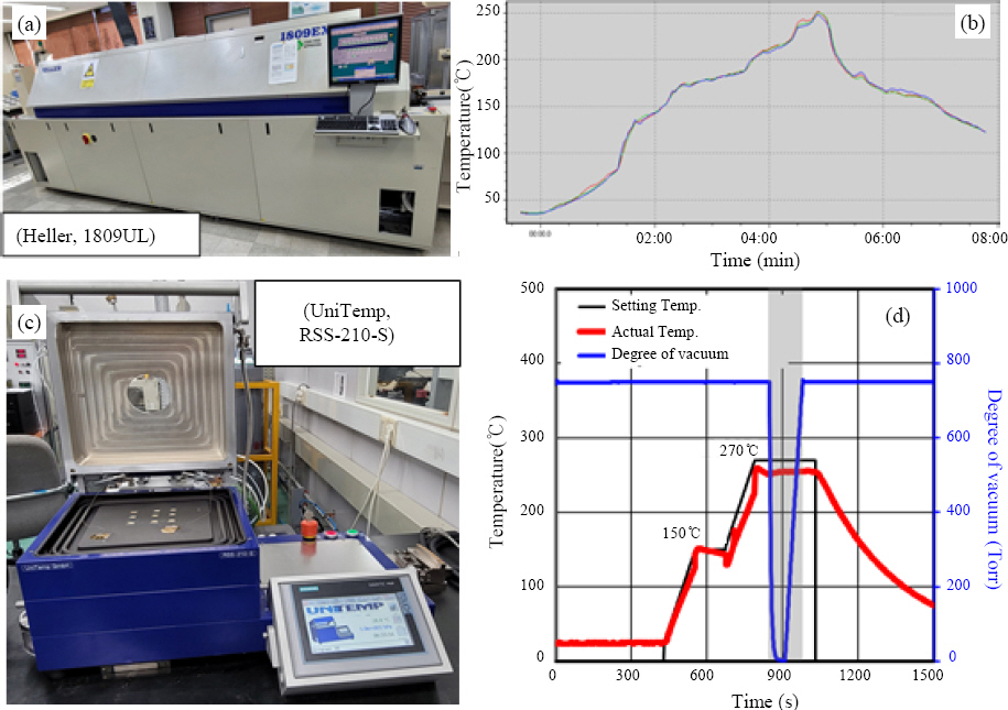
As for the MCC soldering processes performed in the experiment, hot air reflow soldering (Heller Co. Ltd., 1809UL, USA) and Vacuum soldering (Unitemp Co. Ltd., RSS-210-S, Germany) were applied for optimization of soldering process in order to achieve minimization of void defects in the substrate and MLCC joints. Hot air reflow soldering was performed for 8 minutes in total with the preheating temperature of 150-160 ℃ and a maximum temperature of 245-250 ℃ for 30s. For vacuum soldering bonding, the bonding was performed for a total of 17.5 min with the preheating temperature of 150℃ for 120s and the maximum heating temperature at main heating section at 255℃ for 180s with the degree of vacuum at 5 hPa (3.75 torr).
2.4 Measurement of void content at solder joints and shear strength test
The void content measurement of the solder joints was performed based on the area of voids existing within the joint area of the solder, and the void measurement was performed using X-ray non-destructive microscope (Resolution, X-Tek Co. Ltd., UK). Dage 4000 (Nordson Co., Ltd., USA) was used for measurement of the joint strength of the solder joints in MLCC chip components, and shear strength test was performed on the MLCC solder joints. In the shear strength test, the test was performed under the conditions of test speed at 167 ㎛/sec and the height of the test fixture at 50 ㎛ from the substrate, and the bonding strength was comparatively analyzed with respect to the type of solder paste and the type of soldering process used.
3. Experimental Results
3.1 Void content of MLCC solder joints
For MLCC soldering, as shown in Fig. 5, the solder paste was printed on the pad surface of the substrate and the printing state was observed using an optical microscope. After the solder paste was printed on the substrate pad surface, slumps were well formed and maintained. After mounting the MLCC chip on the printed solder paste, the bonding process was performed using reflow soldering and vacuum soldering processes. After the soldering, the observation of the 1005 MLCC and 0603 MLCC joints showed good bonding state of solder fillets as can be seen in Figs. 6 and 7. Fig. 8 shows the comparison of the void content in the joint with different types of solder paste and the soldering processes. The void content (%) of the 1005 MLCC joint bonded by the hot air reflow soldering process was about 1.6-4.3%, and that of the 0603 chip was about 1.1-3.7%. On the other hand, the void content of the 1005 MLCC joint bonded by the vacuum soldering process was 0.1-0.7%, and that of the 0603 chip was 0.5-1.5%. Although the result from the conventional hot air reflow soldering process showed a stable joint void content of less than 5%, the result confirmed that the void content of the joint was significantly reduced with the application of vacuum soldering. As shown in Fig. 4(d), in the vacuum soldering process, a vacuum state is maintained in the main heating section of the temperature profile, which led to the increase in the void fluidity inside the molten solder and decrease in the voids in the solder joints. In general, as the size of the component or the area of the joint becomes smaller, the void content within the molten solder tends to increase due to the application of the greater surface tension on the surface in contact with the pad of the substrate or the solder. For this reason, the result showed that the voids that were not completely removed in the conventional reflow process were effectively removed int eh vacuum soldering process. Also, in the case of the same SAC305 solder, the use of T4 and T7 paste showed the result of almost similar void content, but in the case of 1005 MLCC chip, the use of T7 paste showed rather higher void content. This is considered to be the result of applying the same temperature profile to the T4 and T7 solder pastes, and it is judged that with the decrease in the powder size of the solder paste, applying different temperature condition from the existing T4 is more appropriate. In both SAC105 and SAC0307 solders with the powder size of T4, a similar level of void content at less than 2% was observed.
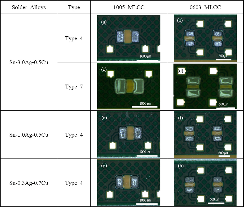
Optical micrographs after printing process with various solder alloys and types, (a-d) Sn-3.0Ag-0.5Cu, (e,f) Sn-1.0Ag-0.5Cu and (g-h) Sn-0.3Ag-0.7Cu solder pastes
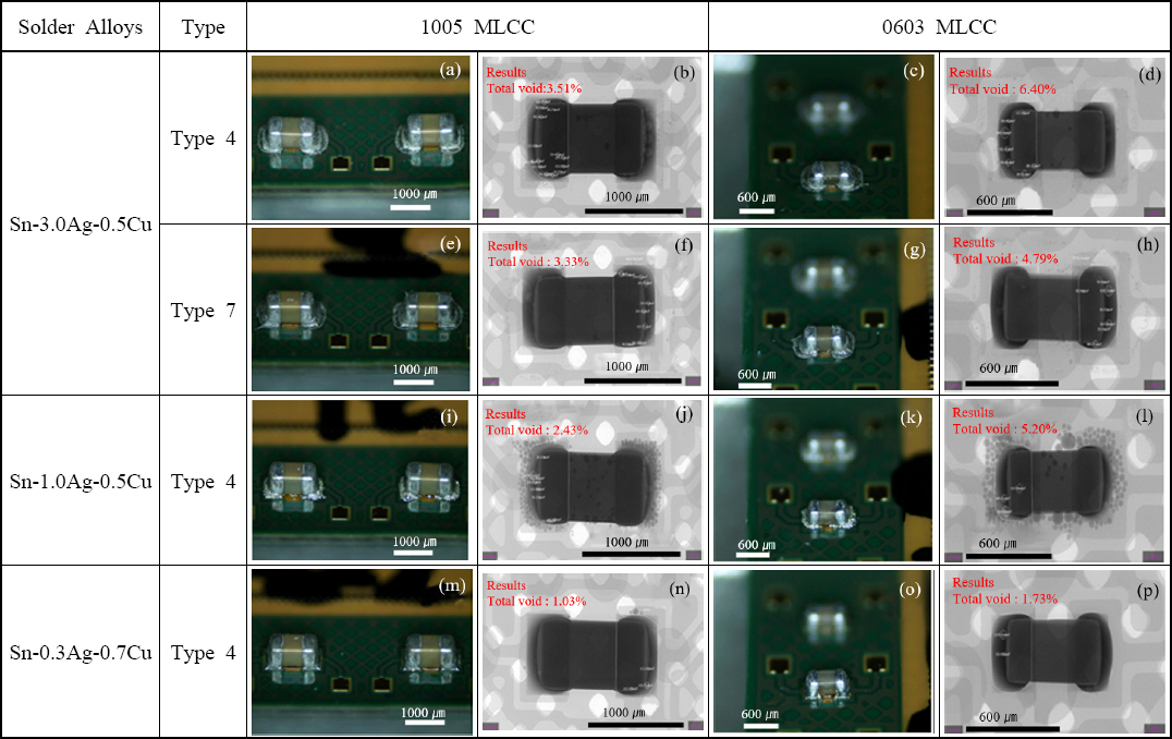
Optical micrographs and X-ray non-destructive void content of 1005 and 0603 MLCC solder joints with (a-h) Sn-3.0Ag-0.5Cu, (i-l) Sn-1.0Ag-0.5Cu and (m-p) Sn-0.3Ag-0.7Cu solder alloys using by hot air reflow soldering process
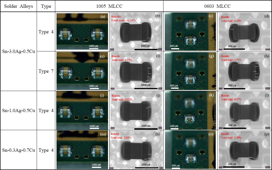
Optical micrographs and X-ray non-destructive void content of 1005 and 0603 MLCC solder joints with (a-h) Sn-3.0Ag-0.5Cu, (i-l) Sn-1.0Ag-0.5Cu and (m-p) Sn-0.3Ag-0.7Cu solder alloys using by vacuum soldering process

Void content comparison between hot air reflow and vacuum soldering process with various alloy compositions and powder size of the solder pastes
3.2 Bonding strength of MLCC solder joints
Fig. 9 shows the average value of bonding strength for four identical 1005 and 0603 MLCC solder joints, respectively, bonded by the conventional hot air reflow soldering and the proposed vacuum soldering processes. The values of shear strength of hot air reflow soldering and vacuum soldering processes using the same T4 SAC305 solder and 1005 MLCC were 1.06± 0.08 kgf and 1.73±0.11 kgf, respectively, and the shear strength for 0603 MLCC was 0.64±0.04 kgf and 0.70±0.02 kgf, respectively, for each type of process. For the T7 SAC305 solder, the shear strength of the 1005 and 0603 MLCC solder joints were measured at 1.43±0.09 kgf (Reflow) and 1.81±0.13 kgf (Vacuum), and 0.52±0.08 kgf (Reflow) and 0.77±0.03 kgf (Vacuum), respectively. Considering that the standard deviation for the shear strength values of all components was around ±0.1 kgf when measured irrespective of the soldering process, the results indicate that the difference in bonding strength occurred due to the difference in the bonding process. The result from vacuum soldering showed higher bonding strength than that of the hot air reflow soldering process.
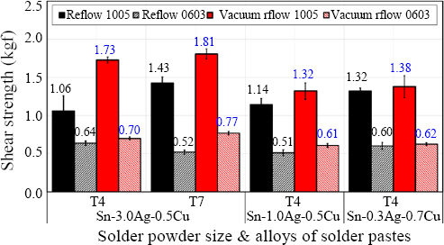
Shear strength comparison between hot air reflow and vacuum soldering process with various alloy compositions and powder size of the solder pastes
Comparing the shear strength according to the difference in T4 and T7 powder sizes in the same SAC305 solder, the results from the hot air reflow soldering were 1.06 and 1.43 kgf, respectively, and the results from the vacuum soldering process were measured at 1.73 and 1.81 kgf, respectively. However, when the same bonding process is applied with the same T4 powder size, the initial bonding strength of the SAC305 solder shows similar values regardless of the Ag content. From these results, it can be seen that when the solder of the same composition was used, application of vacuum soldering exhibited greater bonding strength that the case with the hot air reflow soldering. Also, in the same composition of SAC305, T7 with finer powder consistency showed higher bonding strength than T4.
Also, comparing the shear strength of T4 SAC305, T4 SAC105 and T4 SAC0307, the values of 1005 chip were 1.06-1.32 kgf (Reflow) and 1.32-1.73 kgf (Vacuum), and 0603 chip was 0.51-0.64 kgf (Reflow) and 0.61-0.77. kgf (Vacuum), respectively. This indicates that although these were solder with different content of Ag, in terms of the alloy composition of the solder, the bonding strength of the chip component with the same process and the same powder size was more or less the same for all of the SAC305, SAC105 and SAC0307 solders. This indicates that the initial bonding strength of the solder joint shows a similar level within the content range of 0.3-3.0 wt% of Ag in the Sn-Ag-Cu eutectic alloy system. According to the results of previous studies by Hong7-9), when the content of Ag3Sn in the substrates of SAC305 and SAC0307 solder was compared after 2000 cycles of thermal shock, the Ag3Sn content in the SAC0307 solder was smaller. The previous study reported that with the decrease in the Ag content in the solder substrate, the production of primary-Sn increased and consequently, the amount of Sn to form Ag3Sn decreases, leading to the decreased fraction of Ag3Sn in SAC0307 solder than in SAC305 solder. In this way, it was reported that finely dispersed Ag3Sn contributes to the increase of the initial bonding strength of the solder joint, but when the aging temperature is increased and exposed to high temperature for a long time, the bonding strength of the solder joint is reduced by the growth and coarsening of Ag3Sn7-9).
However, in the soldering processes used in this study, greater shear strength was observed in the vacuum soldering process than in the hot air reflow process, and it can be inferred that the vacuum soldering process reduces the void content and contributes to the increase in the bonding strength of the solder joints. The experimental results compare the difference in initial bonding strength, and it is judged that for comparison of long-term reliability of the solder joints, the difference according to alloy composition and powder size should be compared by a thermal shock test.
3.3 Analysis of solder joint interface
The images of the sectional view for the T7 SAC305 solder joint with the application of hot air reflow process for 1005 MLCC and 0603 MLCC are presented in Fig. 10 and Fig. 11, respectively. The void content of the solder joint was considerably small, and the figures also confirm that the joint fillets were also well formed. It can be seen that in the solder joint interface between the chip and the substrate, (Cu,Ni)6Sn5, the intermetallic compound (IMC) was formed. In general, IMCs of (Cu,Ni)6Sn5 and (Ni,Cu)3nSn4 are formed in the SAC305 soldering interface that has undergone the surface treatment of Electroless Nickel Immersion Gold (ENIG) or ENEPIG. Also, Ni-P IMCs such as NiP, Ni3P and Ni3P4 are formed on the interface of Ni plating layer and solder and in the area of solder joint, the formation of Ag3Sn and Cu6Sn5 have been reported 7,8,10-11). In this study, as can be seen in Fig. 9(b-c), the formation of (Cu,Ni,Pd)6Sn5 and (Ni,Cu,Pd)3nSn4 IMCs was observed in the initial interface after soldering, on the SAC305 solder and ENEPIG joint interface. Fig. 12 shows the SEM micrographs for the sectional analysis of the SAC105 solder joint of 0603 MLCC chip components. In the substrate area of the solder joint fillet, Cu6Sn5 and Ag3Sn, the typical IMCs observed in SAC composition were observed. In the MLCC-ENEPIIG substrate joint interface, the formation of Ni,Cu,Pd)3nSn4 IMC was observed. Also, in the case of ENIG-treated surface, Au-Sn compounds are detected in the substrate12). As Au-Sn IMCs, there are various types of IMCs including AuSn, Au2Sn, AuSn2, and AuSn4, and a trace amount of needle-shaped Au2Sn IMCs was also detected at the joint in Fig. 9(b).

SEM micrographs of 1005 MLCC solder joint with Type 7 Sn-3.0Ag-0.5Cu solder after hot air reflow soldering

SEM micrographs of 0603 MLCC solder joint with Type 7 Sn-3.0Ag-0.5Cu solder after hot air reflow soldering
Fig. 13 shows the sectional SEM micrographs of the SAC105 hot air reflow solder joint of 0603 MLCCsubstrate. In the soldering interface of the MLCC electrode area, irregular needle-shaped IMCs of (Cu,Ni)6Sn5 was formed, and in the junction solder layer, (Ni, Cu,Pd)3Sn4, Ag3Sn, and Cu6Sn5 IMCs were formed. On the interface of the solder-BT substrate, NiP and (Cu,Ni)6Sn5 IMCs were observed. Fig. 14 shows the SEM and EDS analysis of the area in which the interface of the solder-BT substrate is mainly formed. In the solder substrate part, the formation of Cu6Sn5, Ag3Sn and the needle-shaped (Ni,Cu,Pd)3Sn4 IMC was observed, and in the soldering interface of the substrate, the formation of Ni,Cu,Pd)3Sn4, (Cu,Ni)6Sn5, NiP and Ni3P IMCs was confirmed. It has been reported that when various IMCs are formed on the interface between ENEPIG finish substrate and soldering joint of SAC composition, growth behavior of the IMCs over time affects the long-term reliability of the solder joint7,8,10,11). The various IMCs shown in this study contribute to the improvement of the initial bonding strength, but the types of IMCs produced vary depending on the pad surface-treated layers, but almost the same types of IMCs were formed according to the type of the solder and Ag content. However, in the long term, these factors are also thought to induce the degradation in the joints, and therefore, further investigation on the long-term reliability is required.
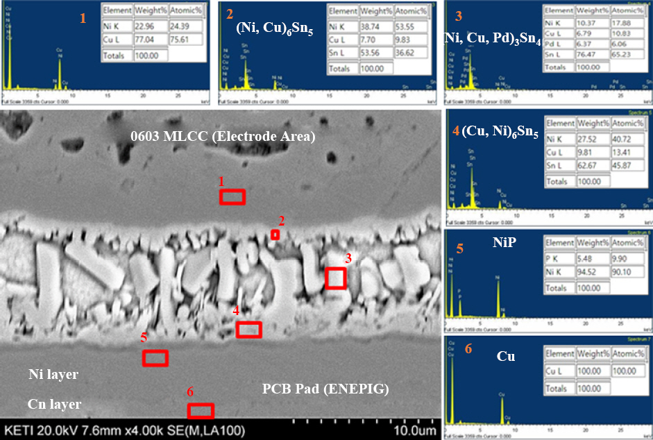
SEM micrograph and EDS analysis results of 0603 MLCC solder joint between BT substrate and MLCC with Type 4 Sn-1.0Ag-0.5Cu solder after hot air reflow soldering
4. Conclusion
In this study, soldering was performed with 1005 and 0603 MLCC components using the SAC305, SAC105 and SAC0307 solder through application of hot air reflow and vacuum soldering process, respectively, and comparative analysis on the void content in the solder joint, shear strength and microstructure was performed. The key findings can be outlined as follows.
1) Although the hot air reflow soldering process showed a stable void content in the joint at less than 5%, the application of the vacuum soldering process markedly reduced the void content of the solder joint. However, there was no significant difference in void content with respect to the powder particle size of the solder in the same bonding process. However, it is expected that if temperature profile suitable for the finer powder can be applied, superior bonding properties can be achieved.
2) In terms of the bonding strength of the SAC305 solder joint under the same powder size condition, the result from the use of hot air reflow soldering showed greater bonding strength than that from the use of vacuum soldering. This indicates that the vacuum soldering process is effective in removing voids during the void joining process, and the reduction in the void content contributed to the enhancement of the bonding strength of the solder joint.
3) With the application of the hot air reflow soldering and vacuum soldering process, the bonding strength of the T4 SAC305 solder joint was slightly higher than that of the SAC105 and SAC0307 solder, but the overall initial bonding strength was similar between the result values. Therefore, within the Ag content of 0.3-3.0 wt%, the effect on the initial bonding strength of SnAg-Cu solder is considered to be at the same level.
4) Various types of IMCs including Cu6Sn5, Ag3Sn, (Ni,Cu,Pd)3Sn4 (Cu,Ni)6Sn5, NiP, and Ni3P were formed on the interface between the ENEPIG finish substrate and SAC solder joint, and these IMCs are considered to contribute to the increase in the initial solder joint strength.
Acknowledgments
This research was conducted with the funding from the Material and Components Technology Development Project (Project number: 20011427) supported by the Ministry of Trade, Industry and Energy.


