Optimization of FC-CSP and MLCC Soldering Process Using Type 7 Solder Paste
Type 7 솔더 페이스트를 적용한 FC-CSP 및 MLCC 솔더링 접합공정 최적화
Article information

Abstract
To confirm the possibility of simultaneous bonding between Si chip and multilayer ceramic capacitors (MLCCs), vacuum reflow soldering is performed between a Si chip and each of 2012, 1608, 1005, 0603, and 0402 MLCCs using Type-7 Sn-3.0Ag-0.5Cu (SAC305) and Sn-0.7Cu solder pastes. To enable an unbiased comparison with the vacuum reflow process, the Si chip and MLCCs are bonded via thermo-compression (TC) bonding and hot air reflow soldering, respectively. The maximum void content of Si chip solder joints bonded via vacuum reflow is 8%. At the MLCC solder joints, the void content yielded by vacuum reflow is lower than that yielded by hot air reflow. The bonding strength of the MLCC solder joint afforded by vacuum reflow is higher than that afforded by hot air reflow. Vacuum reflow is superior to hot air reflow in terms of the void content and bonding strength of the MLCC solder joint. After performing a thermal cycle test (TCT), a crack appeared at the Si chip solder joint bonded by TC bonding. The Cu pillar/Sn-2.5Ag bump is susceptible to cracks after the TCT owing to the insufficient bonding layer thickness yielded; however, the SAC305 sample from vacuum reflow is stable. Meanwhile, (Cu,Ni)6Sn5, Ni3P, and Ag3Sn intermetallic compounds are formed at the MLCC solder joints and then further developed after the TCT. The results of this study indicate the possibility of co-bonding Si chip with MLCCs for semiconductor packaging.
1. Introduction
In a flip chip-chip scale package (FC-CSP), more than 2,000 signal terminals are connected through solder bumps in which a travel path of electrical signals is shorter compared to a wire bonding package (WBP) and a large number of input/output (I/O) can be formed, thus being utilized in a high-density se- miconductor packaging process1). Accordingly, the difficulty of fine pitch soldering process is continuously increasing due to miniaturization and high-density arrangement within a semiconductor package2-5). The probability of defects being generated due to a movement of a device or substrate warpage during a reflow process increases as solder bump pitch decreases; thus, thermo-compression (TC) bonding is used for soldering in order to overcome such issue. However, TC bonding has a disadvantage of reduced productivity from a relatively longer process time since each device is individually soldered6,7). Mostly a Cu pillar/solder bump structure is applied in order to prevent a bridge between bumps in a structure where a solder bump pitch is 150 ㎛ or below7). A Cu pillar/solder bump is formed by placing a hemispherical solder on top of a Cu pillar in which a bridge between solders can be more effectively prevented by minimizing the spreading of a solder when compared to a general spherical solder ball. However, the reliability of a solder joint has been reported to degrade in a high-temperature environment as the thickness of the solder joint decreases since the solder amount is insufficient compared to a conventional solder bump8).
Various package technologies are being developed for high-dimensional structures such as multifunctional, highly-integrated system on chip (SoC), system in package (SiP), package on package (PoP), and embedded package to overcome the limitations of a fine solder bump package. High-performance, miniaturization, and cost reduction are feasible since other packages and electric components such as passive components, micro-electro mechanical systems (MEMS), and optical components can be selectively included depending on applied field9). In general, TC bonding is applied to high-integrated Si chip, while hot air reflow is applied to passive components such as inductor or multi-layer ceramic capacitor (MLCC), and thus, two separate processes are required if highly-integrated Si chip element and passive element are mounted together within one package. Therefore, simultaneously soldering passive components with Si chip having a fine pitch bump of 150 ㎛ or below can be completed in one process, while reliability can be improved by increasing the soldering amount through a soldering process using a solder paste when compared to the conventional Cu pillar/ plated solder bump.
MLCCs are passive components enabling a semiconductor to function smoothly by storing electricity and consistently supplying the amount of electricity required for active components. Approximately 1,000 MLCCs are mounted in smartphones, and between 3,000 and 10,000 in automobiles, while the number of MLCCs required is constantly growing due to the advancement in electric and autonomous vehicle technology10). Thus, the development of micro-size, high-capacity components such as MLCC of 0603 or 0402 ㎜ is in progress. The MLCC is typically soldered through a hot air reflow process. In the hot air reflow process, a void is formed in the MLCC solder joint, and the proportion of a void increases as the size of an MLCC decrease which affects the reliability. In the vacuum reflow process, fluidity of a void is increased when a solid state solder is melted as a vacuum state is maintain in the peak temperature range, and voids can be effectively reduced through vacuum reflow11).
This study, therefore, proceeded with the vacuum reflow process using a solder paste of Sn-3.0Ag-0.5Cu (SAC305) and Sn-0.7Cu (SnCu) having Type 7 particle size for the simultaneous soldering optimization of five MLCCs of 2012, 1608, 1005, 0603, and 0402 mm and Si chip for which a fine pitch solder bump of 150 ㎛ or below is formed. Furthermore, TC bonding and hot air reflow were applied to Si chip and MLCC, respectively, for a comparison with conventional processes; a thermal cycle test (TCT) was performed for verifying the degradation characteristics and soldering reliability of Si chip and MLCC solder joints.
2. Experimental Method
2.1 Experiment Materials
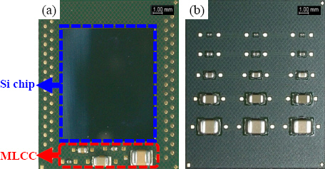
Fig. 1 shows the substrate used in the experiment where electroless-nickel electroless-palladium immersion- gold (ENEPIG) plating is applied to a bismaleimide triazine (BT) substrate of 15 × 15 mm in size and 0.3 mm in thickness. For a solder paste, the alloy composition of Sn-3.0Ag-0.5Cu (SAC305, MK Electron Co. Ltd., Korea) and Sn-0.7Cu (SnCu, SNF Co. Ltd., Korea) having Type 7 particle size was used.
Optical micrographs of BT substrate for (a) Si chip and MLCC and (b) MLCC BT substrate
As shown in Fig. 2, 1,744 Cu pillar/Sn-2.5Ag bumps were applied to a 10 × 10 mm Si chip having 90 ㎛ diameter, 150 ㎛ pitch, and 50 ㎛ (Cu pillar 30 ㎛, Sn-2.5Ag 20 ㎛) height. The thickness and aperture ratio with respect to the joint area of a metal mask used in solder paste printing were set to 30 ㎛ and 50% (Si chip) / 144% (MLCC), respectively, to proceed with printing.
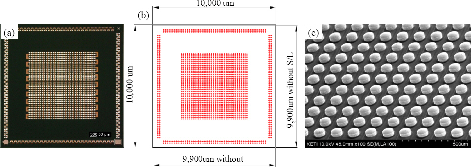
Overview of Si chip: (a) optical micrograph of Si chip, (b) schematic drawing, and (c) magnified SEM image of Cu pillar bump
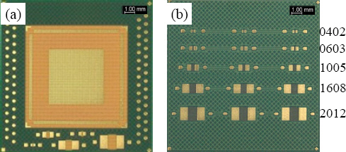
Furthermore, for evaluating the characteristics of MLCC joints according to soldering process and solder paste composition, a substrate shown in Fig. 1(b) was fabricated where five sizes of MLCCs - 2012, 1608, 1005, 0603 and 0402 mm - were used. Printing was proceeded with by using a 50 ㎛-thick metal mask with 144% aperture ratio with respect to the joint area.
As shown in Fig. 3, a printing jig for fine adjustment in a solder paste printing process was fabricated, and a fixing jig was also fabricated to reduce the occurrence of substrate warpage and movement of a device during reflow soldering.
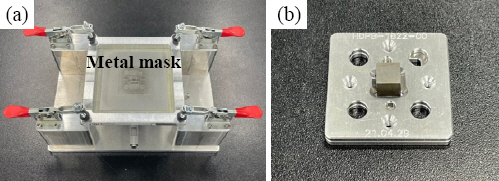
Photographs of (a) solder paste printing jig and (b) reflow soldering jig for fixing the Si chip and substrate
2.2 Vacuum Reflow, Thermal-Compression, and Hot Air Reflow Soldering
For selecting the vacuum reflow process temperature, Si chip soldering was performed by setting the peak temperature to 280℃, 260℃, and 240℃ after printing the SAC305 solder paste. Fig. 4 shows the machine and temperature profile of each process. The vacuum reflow process machine (RSS-210-S, UniTemp Co. Ltd., Germany) had the peak temperature of 245℃ for simultaneous soldering of Si chip and MLCC.
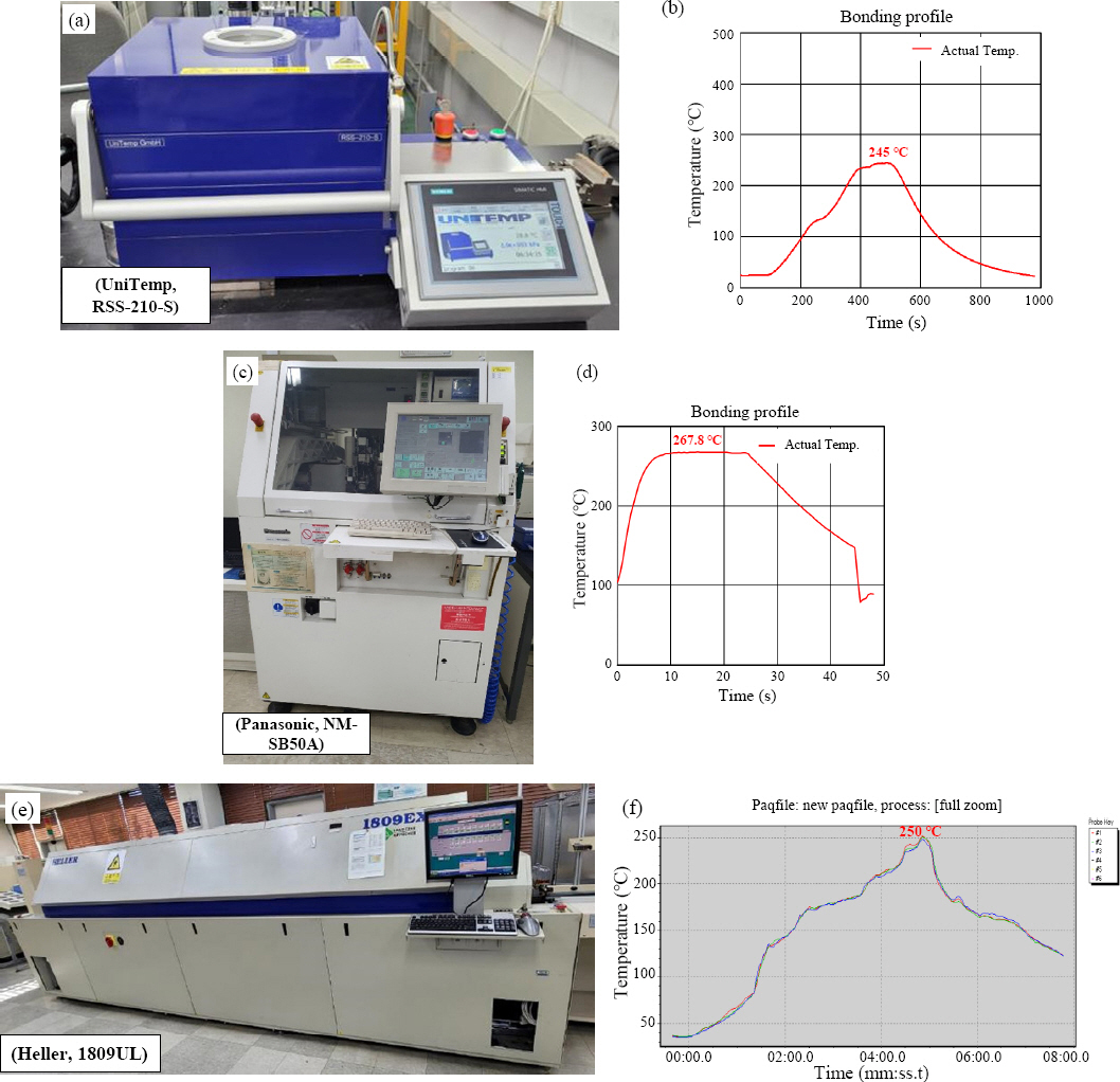
Photographs of (a) vacuum reflow machine and (b) temperature profile, (c) thermal-compression bonding machine and (d) temperature profile, and (e) hot air reflow machine and (f) temperature profile
Flip-chip die attach (NM-SB50A, Panasonic Co. Ltd., Japan) machine was used for TC bonding where Si chip soldering was proceeded at the peak temperature of 267.8℃ under 10 N. A Cu pillar/Sn-2.5Ag bump soldering sample was fabricated through TC bonding for a comparison with the SAC305 sample from vacuum reflow. Electrical resistance of all bumps connected through a daisy chain was measured after soldering to verify the soldering state.
The hot air reflow process machine (1809UL, Heller Co. Ltd., USA) had the peak temperature of 250℃ for MLCC soldering, and a comparative analysis with the MLCC sample from the vacuum reflow process was conducted.
2.3 Solder Joint Void Content Measurement
For measuring the void content of a solder joint, the void area was measured with respect to the Si chip and MLCC solder joint area. The void content analysis was performed using X-ray non-destructive analysis equipment (Resolution, X-Tek Co. Ltd., UK), and the void area was measured using the iSolution program.
2.4 MLCC Solder Bonding Strength Measurement
Shear strength test equipment (Dage 4000, Nordson Co. Ltd., USA) was used to measure the strength of the MLCC solder joint. The shear strength test was performed at the speed of 167 ㎛/second in which the height from the measured jig substrate was set to 300 ㎛ for 2012, 1608 and 1005 MLCC and 100 ㎛ for 0603 and 0402 MLCC.
2.5 Thermal Cycle Test
A TCT was performed to examine the reliability and degradation characteristics of the Si chip and MLCC solder joint. The test was performed in the temperature range between -55 and 125℃ for which a total of 500 cycles were repeated for 10 minutes dwell time at each low and high temperatures.
3. Experimental Results
3.1 Microstructure Characteristics of Joint Per Temperature
When the daisy chain resistance of bumps was measured after soldering, approximately 1 Ω or less of resistance was stably measured in the samples at the set temperatures of 280℃ and 260℃, but no resistance was measured in the sample at 240℃. Fig. 6 shows the Si chip cross-sectional analysis result according to set temperature. Soldering was adequately completed in the sample at the set temperatures of 280℃ and 260℃, but a crack was formed in the sample at 240℃ which indicated defective soldering. Accordingly, the vacuum reflow process was proceeded with at the set temperature of 260℃ in order to proceed with soldering at a low temperature, where the actual peak temperature was around 245℃. Fig. 6(a) shows the result of performing simultaneous soldering of Si chip and MLCC at the peak temperature of 245℃; Fig. 6(b) shows the sample fabricated for evaluating the characteristics of MLCC joint.
Optical micrographs of (a) Si chip and MLCC package and (b) MLCC package after vacuum reflow soldering
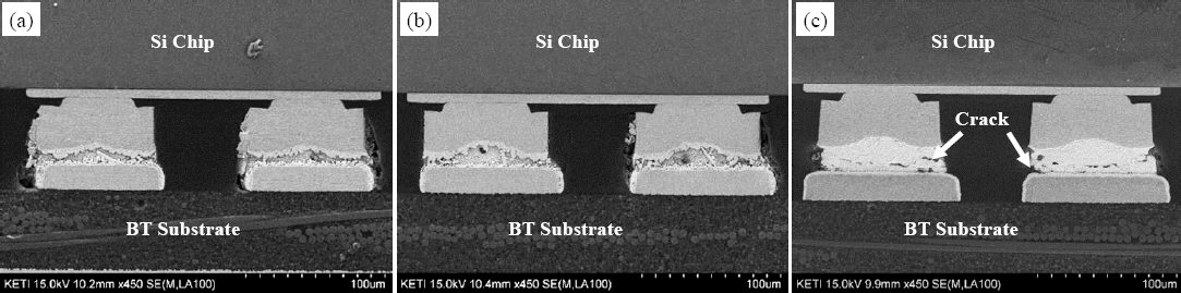
SEM micrographs of Si chip solder joints after vacuum reflow: peak temperature (a) 280 ℃, (b) 260 ℃, and (c) 240 ℃
3.2 Comparison of Void Content in Si Chip and MLCC Solder Joint
As shown in Fig. 7 and Fig. 8, the void at the solder joint was analyzed and measured through an X-ray analysis. Fig. 9 shows the comparative graph of void content of MLCC solder joints between hot air reflow and vacuum reflow processes; the changes in void content with respect to the solder paste can be observed. As illustrated in Fig. 7, the void content of SAC305 was 6.4% in the Si chip solder joint soldered through vacuum reflow, which is less than 7.6% of SnCu. The void content of SAC305 in the MLCC solder joint was less than that of SnCu.
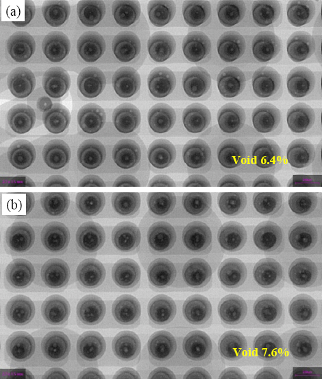
X-ray non-destructive analysis images of Si chip solder joints after vacuum reflow : (a) Sn-3.0Ag- 0.5Cu and (b) Sn-0.7Cu solder alloys
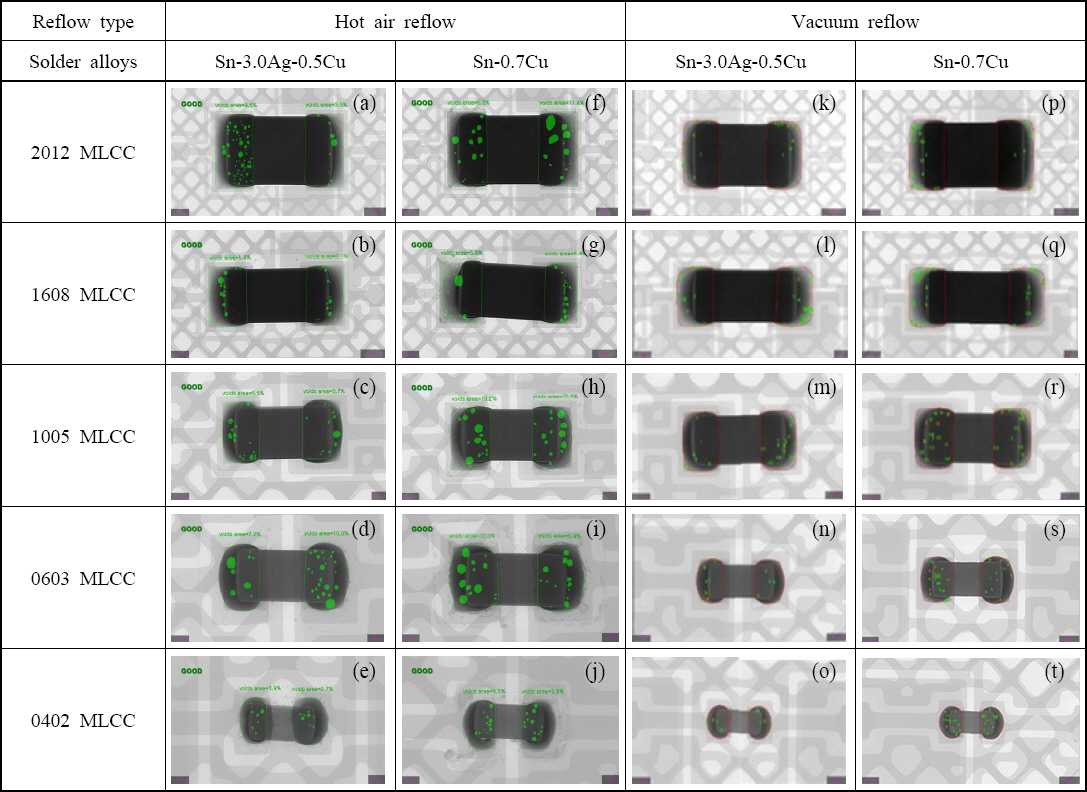
X-ray non-destructive analysis images of 2012, 1608, 1005, 0603, and 0402 MLCC solder joints: (a-e) hot air reflow / Sn-3.0Ag-0.5Cu, (f-j) hot air reflow / Sn-0.7Cu, (k-o) vacuum reflow / Sn-3.0Ag-0.5Cu, and (p-t) vacuum reflow / Sn-0.7Cu
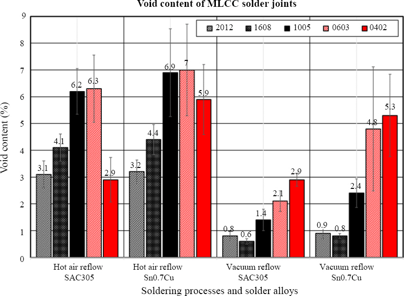
Void content comparison between hot air reflow and vacuum reflow with Sn-3.0Ag-0.5Cu and Sn-0.7Cu solder alloys and various MLCC size
The void content was less than 7% for both hot air reflow and vacuum reflow in the MLCC solder joint, but the void content of vacuum reflow was further decreased than the void content of hot air reflow. In the SAC305 sample of vacuum reflow, the void content was 0.8% in 2012 MLCC and 2.9% in 0402 MLCC, which indicates that the void content is greater in the sample of a smaller MLCC.
SAC305 has a melting point of 217 - 220℃ while SnCu has a melting point of 227 - 229℃ as the same temperature profile was applied to SAC305 and SnCu solder pastes; thus, fluidity of voids in SAC305 increased due to a lower melting point than SnCu, thus exhibiting less void content. The fluidity of voids in the joint was increased by maintaining the vacuum state during the melting process of solder; hence, the void content in vacuum reflow is lower than that in hot air reflow. Since the proportion of void with respect to the solder joint volume increases as the MLCC element size decreases, the void content tended to increase.
3.3 Comparison of Bonding Strength in MLCC Solder Joint
The comparison results of shear strength in the solder joints before and after the TCT are presented in Fig. 10 in which bonding strength decreased after the TCT in all samples. The bonding strength in vacuum reflow was higher than that in hot air reflow, while the bonding strength of SAC305 was slightly higher than that of SnCu in the same soldering process.
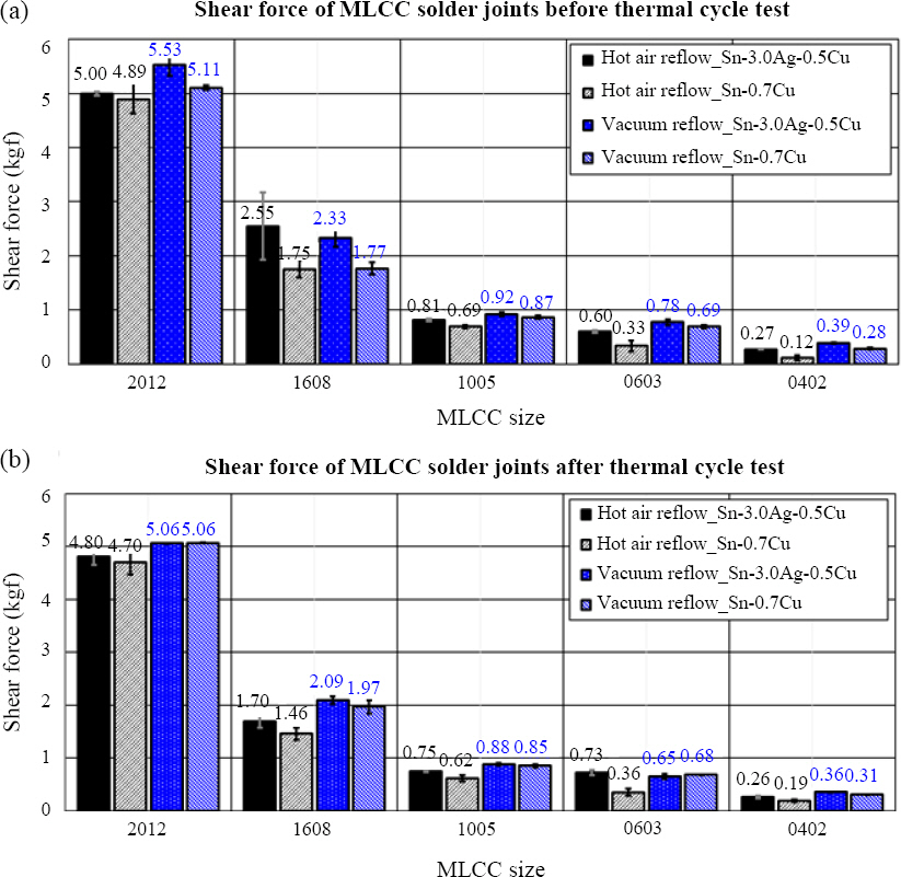
Shear force comparison between hot air reflow and vacuum reflow with Sn-3.0Ag-0.5Cu and Sn-0.7Cu solder alloys and various MLCC size: (a) before thermal cycle test and (b) after thermal cycle test
Substrate warpage occurred due to repeated thermal- mechanical fatigue in high and low temperatures during the TCT, which induced shear stress in the solder joint and ultimately reduced the bonding strength. Main- taining a low void content in the solder joint during vacuum reflow contributed to the improvement in bonding strength. In general, Ag3Sn IMC is finely distributed within the SAC305 solder joint, thus exhibiting higher solder joint strength than SnCu12).
3.4 Microstructure Analysis of Si Chip Solder Joint
The results of scanning electron microscopy (SEM) and energy dispersive spectroscopy (EDS) for the Si chip solder joint are shown in Fig. 11 and Fig. 12, respectively. As illustrated in Fig. 11, soldering was properly formed in all bump solder joint, and warpage was not observed. Cu6Sn5 and (Cu,Au)6Sn5 IMCs were formed in the Si chip solder joint, while (Cu,Ni)6Sn5 IMC was formed in the BT substrate solder joint. The daisy chain resistance value of the Si chip sample soldered through vacuum reflow by applying the SAC305 solder paste was approximately 1 Ω or below, which was fairly stable. Growth and coarsening of IMCs were not significant even after the TCT in the bump solder joint, and the bumps were stably formed throughout. The sample applied with the SnCu solder paste demonstrated similar results as the SAC305 sample. In contrast, the daisy chain resistance value after the TCT in the Cu pillar/Sn-2.5Ag bump sample to which TC bonding is applied was infinite or approximately 1.5-18 Ω, which was unstable, and cracks in the solder joint were observed in the cross-sectional analysis. In particular, the TC bonding sample with an insufficient soldering amount after the TCT was particularly more vulnerable. Therefore, the SAC305 solder bump soldered by vacuum reflow process with a sufficient solder amount after additional solder printing had higher reliability than plated Sn-2.5Ag bump joint.
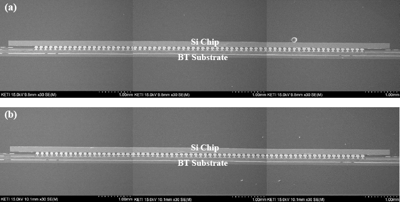
SEM micrographs of Si chip soler joints after bonding: (a) Sn-3.0Ag-0.5Cu sample of vacuum reflow and (b) Cu pillar/Sn-2.5Ag bump sample of thermal compression bonding
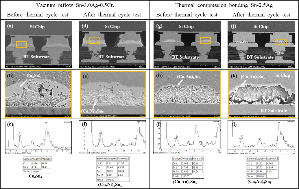
SEM micrographs and EDS analysis results of Si chip solder joints: vacuum reflow soldered Sn-3.0Ag-0.5Cu sample (a-c) and after thermal cycle test (d-f), thermal compression bonded Cu pillar/Sn-2.5Ag bump sample (g-h) and after thermal cycle test (j-l)
3.5 Microstructure Analysis of MLCC Solder Joint
SEM images and EDS results of the solder joint for which 0402 MLCC was applied with hot air reflow using the SAC305 solder paste are provided in Fig. 13. (Cu,Ni)6Sn5 IMC was formed in both MLCC and substrate solder joints. P-rich Ni (Ni3P) IMC layer is formed below the (Cu,Ni)6Sn5 IMC layer of the substrate, and (Pd,Au)Sn4 IMC is formed above the IMC layer. Ag3Sn IMC was finely distributed in the parent soldering material. As illustrated in Fig. 14, IMCs formed above and below the solder joint before the TCT was needle-shaped, and then growth and coarsening of IMCs were observed after the TCT. The EDS analysis results of coarsened IMCs showed that IMC including Pd such as (Pd,Au)Sn4 and (Ni,Pd)Sn4 was formed. The thickness of solder joint IMC was calculated by measuring the area; the IMC thickness of MLCC and substrate solder joint was (a) 5.3 ㎛, (b) 6.5 ㎛, (c) 6.5 ㎛ and (d) 6.8 ㎛ in Fig. 14. According to previous studies, IMC which is brittle became coarsened as the number of cycles increased in the TCT, thus affecting the degradation in the solder joint strength13-15).
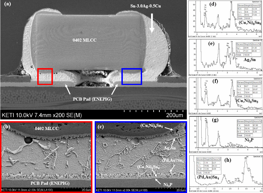
(a-c) SEM micrographs and (d-g) EDS analysis results of 0402 MLCC solder joint with Sn-3.0Ag-0.5Cu solder paste after hot air reflow
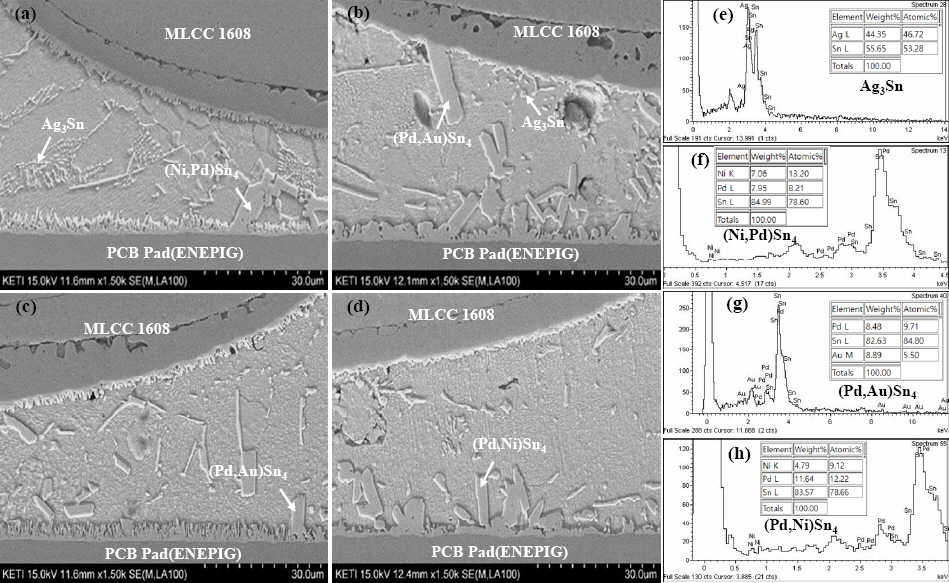
SEM micrographs of 1608 MLCC solder joints after hot air reflow: (a) Sn-3.0Ag-0.5Cu solder paste before thermal cycle test, (b) after thermal cycle test, (c) Sn-0.7Cu solder paste before thermal cycle test, (d) after thermal cycle test, and (e-g) EDS analysis results
4. Conclusion
In this study, simultaneous soldering was performed through the vacuum reflow process for the Si chip for which Cu pillar/Sn-2.5Ag bump was formed and five sizes of MLCCs including 2012, 1608, 1005, 0603, and 0402 using the solder paste consisting of Type 7 SAC305 and SnCu. In addition, TC bonding was applied to the Si chip and hot air reflow was applied to MLCCs for soldering in order to compare the vacuum reflow and conventional processes. The following conclusions have been drawn.
1) When soldering was performed at different temperatures in order to select the appropriate vacuum reflow temperature, soldering was properly completed in the samples at the temperatures of 280℃ and 260℃, and simultaneous soldering was proceeded with at the peak temperature of 260 ℃ through vacuum reflow for low- temperature soldering.
2) The void content in the solder joint of the Si chip was less than 8% in the vacuum reflow process. The MLCC solder joint had less than 7% of void content in both hot air reflow and vacuum reflow, but the void content was further reduced in the vacuum reflow process.
3) When the bonding strength of the MLCC solder joint was measured, vacuum reflow resulted in higher bonding strength than hot air reflow because the reduction in the void content in the vacuum reflow process increased the bonding strength.
4) IMCs of Cu6Sn5, (Cu,Au)6Sn5, and (Cu,Ni)6Sn5 were observed in the solder joint between the Si chip and the substrate. Furthermore, chip soldering reliability can be improved by additionally applying the solder paste for the soldering process of Cu pillar/Sn-2.5Ag bumps. In case of the MLCC, IMCs of (Cu,Ni)6Sn5, Ni3P, Ag3Sn were observed in the solder joint between MLCC and the substrate in which growth and coarsening of IMCs were observed after the TCT.
Acknowledgment
This research was funded by the Materials/Parts Te- chnology Development Program (Project No.: 20011427) of the Ministry of Trade, Industry and Energy.