Growth Behavior of Intermetallic Compounds in Various Solder Joints Induced by Electromigration
Electromigration에 의한 다양한 솔더 접합부에서의 금속간 화합물 성장거동
Article information

Abstract
With the development of the fine pitch technology, the size of the solder bumps contacting the chip and the substrate has decreased, thereby significantly increasing the current density. As a result, intermetallic compounds (IMCs) are formed in solder bumps, and the formation/growth of Kirkendall voids is the main reason for failure, which is accelerated by electromigration. Therefore, various studies have been conducted to restrain the growth of IMCs and Kirkendall voids. This study summarizes the issues that should be considered when investigating the effects of electromigration on solder joints. The prediction and observation of the growth behavior of the IMCs is summarized for various solder bump joints. In addition, we provide an effective method for assisting the fine pitch technology.
1. Introduction
There is an increasing demand for miniaturization and high performance of major products such as smart phones, 3D TVs and computers recently in the electronics industry, and technology for implementing a fine pitch for mounting many devices and terminals in a printed circuit board (PCB) substrate that connects a chip and a main board has been continuously developed in order to satisfy this demand1,2). There was a problem that the current density applied to solder bump increased rapidly as the solder bump that connects the chip and the substrate became finer along with the development of fine pitch technology. The formation and growth of secondary phases induced by electromigration (EM) and thermo-migration (TM) are observed in the solder bump due to the increase in current density and temperature induced by joule heating, and this phenomenon leads to serious problems such as open-circuit failure due to rapid increase in electrical short and electrical resistance in the package3). It has been reported that the formation and growth of Kirkendall voids and intermetallic compounds (IMC) formed between the solder and the substrate, which are the main causes of the problem, is accelerated due to electromigration (EM)4,5). Pb-Sn- based alloys are the alloys that were mainly applied to solder bumps in electronic devices, which have been actively used until 2006. However, studies on Pb-free solders were continuously conducted and solders of various alloys have been developed with the emergence of lead poisoning problems6-8). Although studies have been mainly conducted on intermetallic compounds and Kirkendall void growth behavior in Sn-Ag alloy solder bumpers9,10), studies on the EM effect in solder bump joints of Sn-Cu-based alloys have also been conducted recently11,12).
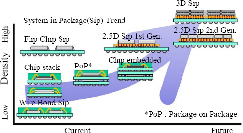
There is a trend of increasing and miniaturization of components mounted in a package due to microminiature fine-pitch technology with the application of Package on Package (PoP) and 3D System in Package (SiP) technologies as shown in Fig. 113-15). It is determined that the structure of the package needs to be changed and the solder bump material needs to be changed for an efficient method to inhibit the formation of defects since the current density applied to the solder bumps is rapidly increasing due to miniaturization. Therefore, the changes of voids and IMC in the joints according to EM effect in solder bump joints of various materials are summarized, and a study that predicts the change in IMC according to EM is introduced in this paper.
2. Experimental and Modeling of Electromigration
The growth of IMC due to EM is observed when a metal atom moves in the movement direction of electron due to an exchange of momentum when a moving electron collides with a metal atom when a current is stressed on the metal interconnect. The driving force of the movement of metal atoms due to EM includes an electron wind force and an electrostatic force. Electron wind force refers to the force that causes electrons that are accelerated by an electric field to collide with a metal atom and transfer momentum to the metal atom to move, and electrostatic force refers to the force that acts on an atom that has lost its valence electron and remains as an ion. Therefore, the effective driving force in EM is given as16),
where J is the EM flux, C is the concentration, D is the diffusivity, Z* is the effective charge number, k is the Boltzmann constant, T is the absolute temperature, e is the quantity of electric charge, ρ is the specific resistance, and j is the current density.
Moreover, the concentration of metal atoms is actually changed according to time. The change in concentration over time is represented by Fick’s second law16).
The thickness of the growing IMC according to the current stressing time by calculating the EM flux at the formed IMC, the solder, and the metal atom can be predicted through Equations (1) and (2). The increase in electrical resistance and electrical short due to voids are indirectly predicted through the growth prediction modeling of IMC since the growth of IMC is related to the formation and growth of Kirkendall voids. The experimental verification is essential in order to verify that the predicted IMC thickness shows the same result when the current is actually stressed. A schematic diagram of current stressing for EM experiments is as shown in Fig. 2a and a schematic diagram of applying a temperature gradient for TM experiments is as shown in Fig. 2b. Sn-0.7Cu is the solder alloy that is used in Fig. 2, and DC source meter (IT6153) of ITECH was used as a power supply. The IMC is grown by stressing a current for a certain period of time through a power supply after constructing the EM experiment set as shown in Fig. 2a. Subsequently, an experimentally verified modeling result was produced by comparing the actual measured thickness of the IMC with the thickness of the IMC that is calculated through modeling.

3. Results & Discussion
3.1 Selection of Pb-free solder alloy
It is required to apply an eco-friendly Pb-free solder alloy with a melting point similar to that of Sn-Pb-based solder (~183 °C) and good electrical and mechanical properties as a consideration when selecting a Pb-free solder alloy. Currently, a variety of Sn-based solders that can replace Sn-Pb based solders are on the market, and Sn-Ag-Cu, Sn-Ag, Sn-Cu, Sn-Zn, and Sn-Bi-based solders are the most common Pb-free solders18). Most Pb-free solder alloys consist of Sn as the main com- ponent and trace amounts of Ag, Cu, Zn, In, and Bi components19).
The eutectic point of the Sn-Zn-based eutectic com- position solder is 199 °C, which has the advantage that the conventional processor can be applied as it is since the melting point is similar to that of the conventional Sn-Pb solder, and it has high strength, and good creep characteristics and thermal fatigue resistance. However, the commercialization is limited since it has fast reactivity with oxygen and the wettability with the substrate is poor20). It has been reported that the oxidation resistance can be improved by adding a trace amount of Ag and Cu since there is a disadvantage that the oxidation is accelerated although the wettability can be improved when a small amount of Bi is added to the Sn-Zn eutectic alloy 21).
The eutectic composition of Sn-Cu-based solder is Sn-0.7Cu and the eutectic point is 227°C. The solder is deformed due to fatigue properties since Sn-0.7Cu solder has lower creep strength than Sn-Ag alloy, and studies and use have been increasing recently since it has been reported that the deformation of the solder resulting from the warpage defect due to the difference in the coefficient of thermal expansion between the chip and the substrate has excellent crack resistance in electronic packages22).
The eutectic composition of Sn-Ag-based solder is Sn-3.5Ag and the eutectic point is 221°C. The increase in the applied temperature of Sn-Ag solder tends to decrease the surface tension and contact angle. Since the surface tension of Sn-Ag solder is higher than that of Sn-Pb and the contact angle is also high23) it has been reported that Sn-Ag solder has lower wettability than that of Sn-Pb solder24). For compensation, it has been reported that adding a trace amount of Cu to Sn- Ag can improve the wettability and fatigue properties, and adding a trace amount of Bi improves the wettability25,26).
Currently, Sn-Ag-Cu-based solder is mainly applied in soldering and it can be defect generation and propagation sites since coarse Ag3Sn phase is formed when the content of Ag is increased. Therefore, Sn-3.0Ag-0.5Cu solder with a melting point of 217 °C has been established as a representative solder that can replace Sn-Pb based solder27).
3.2 Causes and characteristics of EM phenomenon in solder joints
The metal atoms in the solder generally have a strong flow along the movement direction of electrons due to temperature rise when a current is stressed to a solder joint, and the IMC on the anode side grows rapidly as this flow of atoms becomes a driving force and movement of atoms in the same direction is activated. On the contrary, voids are formed by being accumulated on the cathode side, which leads to electrical short due to the growth of the voids and generation of cracks, since the diffusion rate of atoms around the vacancy is relatively reduced. This is a problem caused by the EM phenomenon and a schematic illustration of the EM phenomenon is as shown in Fig. 328). In addition, the internal temperature rises to 100°C or above due to the joule heating effect in the joint and the degradation phenomenon induced by EM is accelerated due to the current crowding phenomenon which is generated by structural problems of the solder joint. Therefore, it is difficult to predict the reliability of the solder joint lifespan, and many studies are being conducted to improve the joint lifespan. The studies that covered the effect of EM phenomenon on each solder joint are summarized in Table 1. The IMC formation behavior of the joints by solder material according to EM is described from the next section.


Previous studies on EM for various solder joints

3.2.1 Characteristics of Sn-Zn solder joints
The microstructure of the Sn-9Zn alloy is as shown in Fig. 4. The as-cast solder of Sn-9wt%Zn eutectic composition did not form intermetallic compounds (Fig. 4a), and the microstructure of this alloy has a structure in which needle-like α-Zn is finely dispersed in a matrix of β-Sn phase29,30). Moreover, oxidation resistance is significantly reduced when the Zn-rich phase is increased in Sn-Zn solder since ZnO is formed due to high reactivity with oxygen of the Zn element as shown in Fig. 4b19). A method to control the formation of ZnO is required in order to improve the bonding characteristics of Sn-Zn solder.
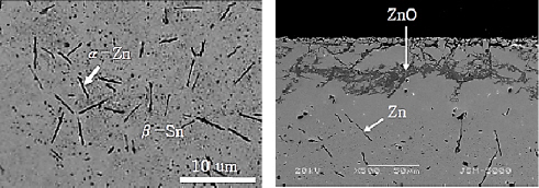
Microstructure of Sn-9Zn alloy20): (a) the shape of each phase, (b) the formation of ZnO
Xue31) observed the growth and component behavior of IMC through energy-dispersive spectroscopy (EDS) line/spot analysis, and Guo32) analyzed the IMC behavior of the solder/Cu substrate interface by adding Ag as a method to improve the oxidation resistance of Sn-Zn solder. The components of the IMC layer between Sn-9Zn solder and Cu substrate (Sn-9Zn/Cu), and the growth behavior of IMC with increasing Ag content and aging time, respectively, are as shown in Figs. 5a and 5b. The IMC layer between Sn-9Zn solder and Cu substrate is mainly composed of CuZn5and Cu5Zn8 (Fig. 5a), and the possibility of lowering the reliability of the solder joint is increased as the Sn component is decreased and the Zn component is increased significantly in the IMC layer through the EDS line analysis31). Therefore, the formation of ZnO was suppressed by adding Ag which has good reactivity with Zn in order to improve the oxidation resistance of Sn-9Zn. The IMC layer that is formed at the interface between the Sn-8.5Zn solder and the Cu substrate is composed of AgZn3 and Cu5Zn8 due to the addition of Ag as shown in Fig. 5b, and the IMC layer of Cu5Zn8 tends to be decreased as the addition amount of Ag is increased, while the IMC layer tends to be increased as the aging time is increased32).

Zhang33) observed changes in the thickness of the anode and cathode sides of the IMC over time (0, 36, 72 and 166 h) with a current density of 3.87 × 10³ A/ cm2 at 150 °C, and the results are as shown in Fig. 6. The IMC layer tended to be decreased at 166 h of current stressing although the IMC layer thickness of Cu5Zn8 was increased at the anode side until after 72 h of current stressing depending on the aging time. The tendency to decrease after 166 h shows the opposite result from the general thermal effect although the increase in the thickness of the IMC layer is induced with the aging time. Moreover, the thickness of the IMC layer was increased until after 72 h of current stressing on the cathode side similar to the anode and the IMC thickness was increased sharply to about 5.4 ㎛ after 166 h (Fig. 6h). The thickness of the IMC layer on the anode side was reduced to about 3.2 ㎛ (Fig. 6g). The formation of the thicker IMC layer on the cathode side is generally the opposite of the “polarity effect” and it has been reported that such a case of reverse polarity is often observed34,35). Zn affects IMC formation in Sn-Zn system. Sn atoms move to the anode due to electron wind force when current is stressed. On the contrary, it is determined that reverse polarity is observed since the back stress acts and the Zn atoms move toward the cathode.
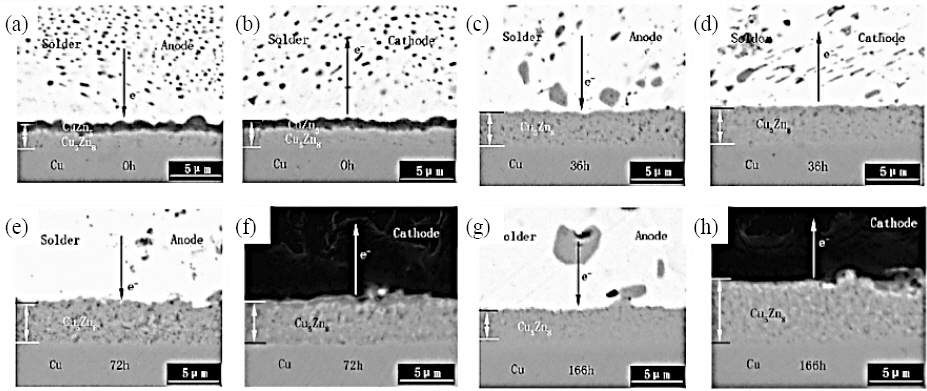
Fig. 6 SEM images of IMCs at the anode (left column) and the cathode (right column) for a current density of 3.87 × 10³ A/cm2 and 150 °C: (a,b) 0 h, (c,d) 36 h, (e,f) 72 h, and (g,h) 166 h33).
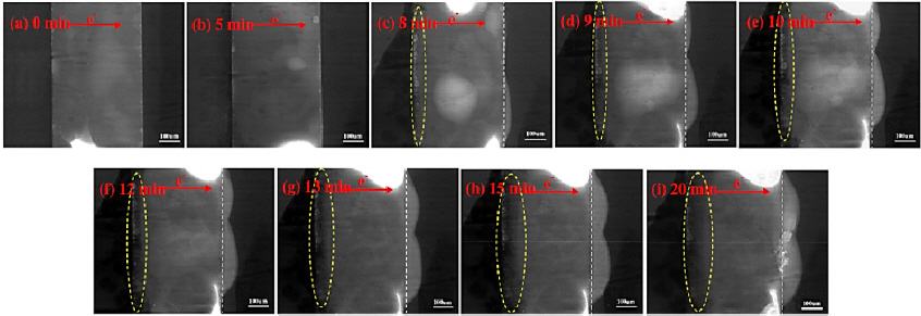
Huang36) observed the change in the thickness of the IMC layer due to liquid-solid electromigration (L-S EM) according to the current stressing time at 250 °C with a current density of 1.2 × 10⁴ A/ cm2 through in- situ images and the results are as shown in Fig. 7. First, air bubbles were slightly formed at the solder interface and the solder began to melt before the current is stressed (0 min) (Fig. 7a), and continuous IMC layers were formed at each interface of anode and cathode after 5 min of L-S EM (Fig. 7b). After 8 min, the IMC layer of the anode marked with a white dotted line was dissolved or Cu was consumed although IMC was grown at the cathode-side interface that is marked with a yellow circle. In addition, the IMC layer that is formed at the anode side interface was extremely thin although the IMC layer that is formed on the cathode side grew thicker up to the Sn-9Zn solder as the L-S EM time increased. These results show that the dissolution of Cu on the anode side is accelerated although the growth of the IMC layer is induced due to the limited consumption of Cu on the cathode side.
Kuo37) observed the IMC behavior that is formed at the Sn-9Zn solder and Cu interface on the anode side through the TEM image of the specimen that is prepared with focused ion beam (FIB) after 100 and 185 h of stressing current at 130 °C with a current density of 1.0 × 10³ A/cm2 as shown in Fig. 8. Huang36) mechanically explained the accelerated dissolution and consumption of Cu on the anode side as shown in Fig. 8. The behavior and mechanism of IMC formation at the solder/Cu interface on the anode side with 100 h of current stressing are as shown in Figs 8a and 8b. A layered Cu5Zn8 IMC in the longitudinal direction was formed at the solder/Cu interface on the anode side and the IMC of Cu6Zn5 was observed at the Cu5Zn8 IMC/Cu interface (Fig. 8a). The Sn atoms move rapidly through the γ- Cu5Zn8 crystal grain boundary due to EM since the grain boundary of γ- Cu5Zn8 phase in the longitudinal direction is almost parallel to the movement direction of the electrons when a current is stressed. Therefore, IMC of Cu6Sn5 is formed through the accumulation of Sn and the interaction of Cu at the Cu5Zn8 IMC/Cu interface on the anode side (Fig. 8b). The consumption of Cu on the anode side is relatively severe due to the growth of the Cu6Sn5 IMC layer after 185 h of current stressing (Fig. 8c). Since the diffusion of Cu in Sn is more dominant than the diffusion of Sn in Cu, it is formed in the Cu layer on the anode side after forming Cu6Sn5 IMC at the Cu5Zn8 IMC/Cu interface as Sn moves to the Cu layer on the anode side through EM, thereby explaining the consumption of Cu (Fig. 8d).

3.2.2 Characteristics of Sn-Cu solder joints
The microstructure of Sn-0.7Cu alloy is composed of β-Sn and Cu6Sn5/β-Sn eutectic composition, and the microstructure of this alloy is as shown in Fig. 938). Hung39) observed the microstructure change in Sn-xCu according to the Cu content, and the β-Sn phase tended to become finer although the IMC of Cu6Sn5 was increased as the Cu content was increased. An appropriate addition is required since the melting point of the solder is also increased significantly depending on the Cu content although a large amount of IMC that is evenly dispersed in the matrix serves as a strengthening mechanism. In addition, Yang40) and El-Daly41) conducted studies to improve the electrical/thermal conductivity and solder joint properties of the solder joint by adding Al and Ag components to the Sn-0.7Cu alloy, and observed that the fraction of various IMCs increased and the β-Sn phase became finer.
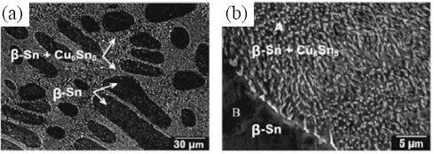
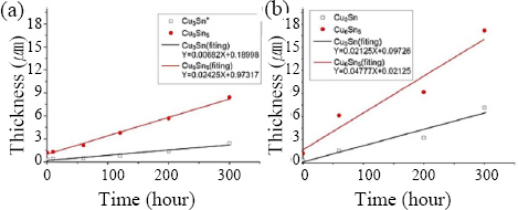
Baek17) observed the effects of EM and TM that are related to the formation and growth of IMC in the solder joint of Sn-0.7Cu. The specimens were prepared for accurate implementation of current straightness and temperature gradient, and were compared with the results of IMC growth modeling. The change in IMC thickness due to EM after 0-300 h of current stressing with a constant current of 6 A and a current density of 10 kA/ cm2 at 120 °C is as shown in Fig. 10a. The IMC layer that is formed at the Sn-0.7Cu/Cu interface is mainly composed of Cu6Sn5 and Cu3Sn, and the IMC layer became thicker as the current stressing time is increased. In particular, the growth of IMC and void showed a close correlation with the electrical short since the void fraction at the interface between the IMC layer of Cu6Sn5 and the Sn-0.7Cu solder was increased simultaneously after 200 h of current stressing. The change in the thickness of the IMC layer due to TM after maintaining the temperature for 0-300 h under heating and cooling conditions of 55/150 °C is as shown in Fig. 10b. The IMC formed at the solder/Cu interface due to TM is composed of Cu6Sn5 and Cu3Sn as shown in Fig. 10a, and the IMC layer tends to be slightly increased as the temperature holding time is increased. However, it was observed that EM has a greater influence than TM on the thickness change in the IMC layer that is formed at the solder/Cu interface. Heo42) observed the IMC growth behavior according to the current density and stressing time at the solder joint that connects the Cu land of the Si wafer and the electroless nickel-immersion gold (ENIG) of the substrate, and the schematic diagram of the solder joint and the method of measuring the IMC thickness are as shown in Figs 11a and 11b, respectively. The change in IMC thickness growing at the interface of the solder joint after 0-300 h of current stressing at 150 °C with current densities of 1.3 × 10⁴ A/cm2 and 1.9 × 10⁴ A/cm2 are as shown in Figs. 12a and 12b, respectively. As a result of the experiment on the change in the thickness of IMC according to the current density and stressing time, Cu3Sn and Cu6Sn5 IMC were grown as the current stressing time was increased and the growth rate of Cu6Sn5 IMC was faster than that of Cu3Sn. In addition, the growth rate of IMC was observed to be about 2-3 times, which is higher than the current density increase rate of 1.5 times, as the current density was increased from 1.3 × 10⁴ A/cm2 to 1.9 × 10⁴ A/cm2. Therefore, it was found that the aging and TM effects due to Joule heating effect need to be considered in addition to EM in the phenomena related to the growth of IMC when the current density is increased42).


3.2.3 Characteristics of Sn-Ag solder joints
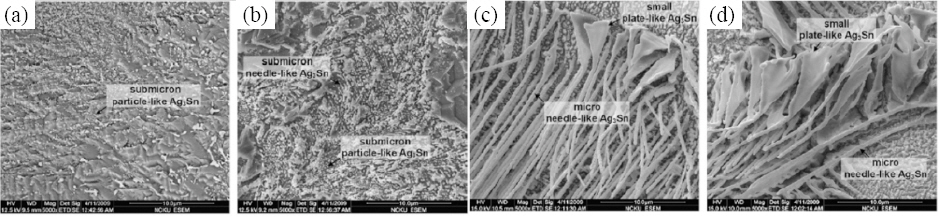
Sn-3.5wt%Ag eutectic alloy is composed of almost pure β-Sn and ε-Ag3Sn phase microstructure. The needle- like Ag3Sn grows along the solidification direction in Sn-matrix according to the two-stage (CR1-CR2) cooling, and nucleation is promoted if the cooling rate is increased during soldering (P1), which hinders the growth of Ag3Sn and shows a finely dispersed structure as shown in Fig. 1343). It has the greatest mechanical strength in the eutectic composition of 3.5wt%Ag with the dispersion strengthening effect due to the characteristics of the finely dispersed ε-Ag3Sn phase25). The IMC layer between the Sn-3.5Ag solder and the Cu substrate (Sn-3.5Ag/Cu) is mainly composed of Cu3Sn and Cu6Sn5, and there is an Ag3Sn phase dispersed in a fibrous form. The study results that are related to the effect of the Ag content and reflow temperature in the solder on the IMC behavior in Sn-Ag solder joints are as shown in Fig. 14. It has been reported that the average number of grains of Cu6Sn5 is increased as the concentration of Ag is increased and the grain width is decreased as the reflow temperature is decreased44).

Jung45) investigated the growth behavior of IMC and Kirkendall voids on the anode and cathode sides according to the current stressing time of the Cu/Sn-3.5Ag/Cu junction. The IMC growth behavior of the Sn-3.5Ag/ Cu solder interface with time variation of 0-200 h without current stressing at 150 °C is as shown in Fig. 15. The main IMCs, Cu3Sn and Cu6Sn5 layers, were grown as the aging time was increased, and most of the Kirkendall voids were formed at the Cu3Sn/Cu interface after 100 h of aging. The increase in aging time causes continuous nucleation and growth of voids, and voids completely cover the Cu3Sn /Cu interface after 200 h. The position of the void formed at the Cu3Sn /Cu interface is moved to the Cu3Sn/Cu6Sn5 interface after 400 h. The reason is that Cu3Sn is converted to Cu6Sn5 and new Cu3Sn is formed at the Cu6Sn5/Cu interface.
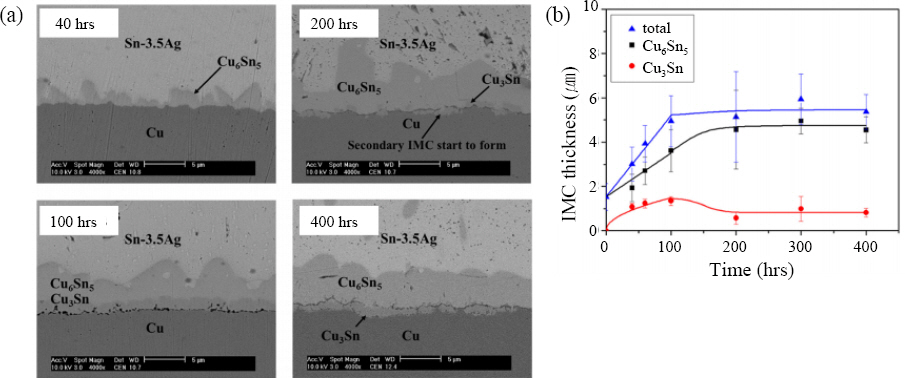
The IMC growth behavior and Kirkendall void fraction of anode/cathode after 40-150 h of current stressing at 150 °C with a current density of 1 × 10⁴ A/cm2 are as shown in Fig. 16. It was found that EM had a polarity effect not only on the thickness of the IMC but also on the fraction of Kirkendall voids. The polarity effect of the IMC thickness is mainly caused by Cu6Sn5 since there is no significant difference in thickness of Cu3Sn depending on the current stressing time, and the growth rate on the cathode side is reduced although the growth of IMC and void is accelerated on the anode side. The formation and growth behavior of Kirkendall voids according to the current stressing time on the anode side were almost similar to the case where there was no current stressing. However, the voids were formed at the Cu3Sn /Cu interface on the cathode side, while Kirkendall voids accounted for most of the Cu6Sn5/Sn interface after 100 h, and the micro cracks were formed at 150 h since the Kirkendall void was saturated at the Cu6Sn5/Sn interface. It has been reported that the formation and growth of Kirkendall voids affect the lifespan of the solder joints3).

3.2.4 Sn-Ag-Cu solder joint characteristics
Sn-3.5wt%Ag-0.7wt%Cu eutectic alloy generally has a microstructure similar to that of Sn-3.5Ag alloy. There is a crystalline phase of η-Cu6Sn5 in the eutectic phase of β-Sn and Sn/Ag3Sn, and in the ε-Ag3Sn phase, which are constituent structures, due to the addition of a trace amount of Cu as shown in Fig. 1746). Therefore, Sn-3.0Ag-0.5Cu alloy has been established as a representative alloy in order to prevent the formation of coarse Ag3Sn phases in a composition with high Ag content.

The IMC layer between the Sn-3.0Ag-0.5Cu solder and the Cu substrate (SAC305/Cu) is mainly configured of Cu3Sn and Cu6Sn5, and there is a eutectic phase of Sn/Ag3Sn as shown in Fig. 18a47). SEM images and schematic diagrams of the microstructure changes at the boundary of the IMC layer/matrix according to the cooling method (cooling rate) are as shown in Figs. 18b and 18c. The size and fraction of Ag3Sn and Cu6Sn5 intermetallic compounds in the matrix are reduced due to the fast cooling rate, and the IMC (Cu6Sn5) layer in the SAC305/Cu boundary is also reported to be reduced48).

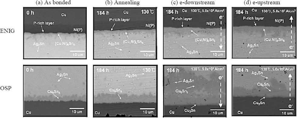
Kim49) investigated the effect of heat treatment according to the upper/lower part of the SAC305 solder joint and the behavior growth of IMC due to current stressing. Immediately after soldering, IMCs of (Cu,Ni)6Sn5, and Cu6Sn5/Cu3Sn were formed at the joint interface in the ENIG surface finish of the upper joint and in the organic solderability preservative (OSP) surface finish of the lower joint, respectively (Fig. 19a). The IMC of Cu6Sn5 and Cu6Sn5 in OSP grew thicker than (Cu,Ni)6Sn5 in ENIG under the heat treatment condition of 130 °C for 184 h, (Fig. 19b) due to rapid diffusion of Cu in a high-temperature atmosphere and rapid growth of the IMC phase of Cu6Sn5. IMC growth behavior according to the electron direction after 184 h of current stressing at a current density of 5.0 × 10³ A/cm2 at 130°C is as shown in Figs. 19c and 19d. The thickness of the IMC tended to be increased as the current was stressed, and thick Cu6Sn5 was observed in OSP although thin (Cu,Ni)6Sn5 IMC layer was formed in ENIG regardless of the electron direction. In the case of downstream electron, the Cu6Sn5 IMC layer was formed thicker by about twice that of the case of upstream electrons. This is because IMC is generated due to diffusion of solder and Cu, and Cu in the solder is accumulated at the interface on the OSP side due to the electron direction in the case of downstream electrons. This IMC growth behavior is caused by the polarity effect due to EM50). It also changes the difference in the diffusion degree of the type of surface finish. In the case of the ENIG surface finish, the plated Ni layer acts as a diffusion barrier layer for Cu to suppress the diffusion of Cu. Therefore, IMC grew less than that of OSP surface finish in the case of ENIG surface finish.
There is a problem in general that the rapid formation of IMCs such as Cu6Sn5 and Cu3Sn due to the rapid reactivity with the solder reduces the reliability of the junction in the junction between the Cu substrate and the SAC30549). Ni plating technology, which acts as a diffusion barrier layer, is being applied in order to improve this problem, and Electroless Nickel Immersion Gold (ENIG) and Electroless Nickel Electroless Palladium Immersion Gold (ENEPIG) plating layer are mainly being used51,52). This surface finish affects the reliability of the package, and furthermore, it has a substantial correlation with the lifespan of the package. Therefore, ENIG and ENEPIG surface finishes are used as UBM (under bump metallization) materials in the fine pitch flip chip process recently due to their good wettability and electroless plating characteristics, and outstanding diffusion barrier characteristics.
3.3 Future trend of solder joint technology deve- lopment
Since a bonding process such as soldering is performed on the PCB surface finish layer in the electronic packaging, the weldability and long-term reliability of the package itself are significantly affected by the surface finish characteristics. The surface finish method of the substrate rather than the type of solder has an important influence on EM since Sn is the main alloying element in various solder alloys. Although the repre- sentative surface finish methods include Cu OSP, hot air solder leveling (HASL), immersion tin, immersion silver, and ENIG and ENEPIG, the ENIG and ENEPIG surface finishes which are the electroless plating technologies, are mainly used rather than the surface finish in which the Cu substrate is directly exposed53,54). In particular, it has been reported that the ENEPIG surface finish layer is better than ENIG in metallurgical and mechanical reliability. The reason is that it suppresses the formation of IMC and Kirkendall voids of Ni3Sn4 and Ni3P due to the Pd layer between the Au and Ni layers of the ENEPIG layer55). However, there is a problem that the gap between solders is decreased and the occurrence of defects due to the increased electrical resistance is increased in order to satisfy the accelerated fine pitch technology since the conventional ENEPIG surface finish is thick with about 3-7 ㎛-thick Ni56). A thin surface finish technology with less than 1 ㎛-thick Ni is being developed (Fig. 20) and various studies are being conducted in order to solve these shortcomings56,57).
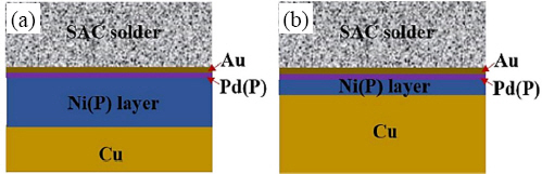
Schematics of surface finishes: (a) normal- and (b) thin-ENEPIG
The thin ENEPIG surface finish has good applicability to fine pitch technology and can be applied not only to soldering but also to various bonding methods. In addition, it is expected to expand the scope of app- lication for R&D as it has good thermal resistance and plating adhesion, and furthermore, reduces the process price58). Many research institutes are currently conducting studies on the properties of solder joints with ENEPIG surface finish of less than 1㎛ applied, and commer- cialization is slow due to problems with reliability and lack of experience in the development field although advanced package manufacturers have entered the test stage for mass production applications.
In addition, the EM phenomenon at the Pb-free solder junction has the closest relationship with the nucleation and growth rates of IMC and void. The stress-migration induced by TM effect and stress, and the warpage phenomenon caused by the stacking of packages in addition to the EM phenomenon need to be considered since the TM effect of increasing the temperature due to Joule heating in the solder joint is increased remarkably as the current density is increased. It is determined that the reliability for the life of the package can be further improved by considering the above.
4. Conclusions
There are challenges that must be overcome technolo- gically with the advent of the next-generation packaging era beyond the current packaging technology. Although the defects due to EM phenomenon among them, which have the greatest effect on solder joints, have been reported so far, they are recognized as the most practical problems due to changes in requirements resulting from miniaturization and high density of packages. In summary, the following problems and improvements are presented.
1) The studies on EM phenomena in various solder joints are being conducted as solder became Pb-free. It is determined that the application of Pb-free solder has stronger resistance to EM phenomenon than Sn-Pb solder according to the previously reported research data61). It is believed that the problem with the EM phenomenon can be solved once additional studies such as the nucleation and growth rate of IMC and void due to EM phenomenon in various Pb-free solder joints, EM rate prediction due to variables such as current density and stressing time, and the effect of Sn growth direction on EM phenomenon are conducted.
2) Various study equipment have been used to conduct these studies, and analyses that applied the latest equipment such as analysis of IMC behavior over time through in-situ images and identification of mechanisms for IMC behavior through TEM analysis have been conducted recently, and these analyses can improve the reliability of study results on solder joints.
3) A number of studies have been conducted on various joints so far, and although solder/ENEPIG is known to have the best bonding characteristics when applying ENEPIG surface treatment substrates, research to reduce the Ni layer of ENEPIG to less than 1 ㎛ is being conducted to satisfy the accelerated micro-pitch technology. However, various research and development must be conducted since it is currently in the test phase for mass production application. Therefore, it is expected the development for solder joints will be intensively researched through the method of reducing the Ni layer of ENEPIG in the future.
4) In accordance with the era of the 4th industrial revolution, modeling studies and warpage studies that can predict the experimental results of the growth of IMC layers and Kirkendall voids due to EM and TM at the interface between ENEPIG and solder are essential.
Acknowledgment
This work was supported by the Technology Innovation Program - Materials and Components Development Program (Grant No. 20011427) funded by the Korean Ministry of Trade, Industry, and Energy (MOTIE) and Competency Development Program for Industry Specialists of Korea Institute for Advancement of Technology (KIAT) (Grant No. P0002019) in the Republic Korea.