
1. Introduction
The key devices for the 4th industrial revolutions are modules of artificial intelligence, augmented reality, internet of things, cloud computing, autonomous vehicles, system integration, and so on. From a packaging technology standpoint, are the packaging technologies required for the above modules that contain these devices ready? The technologies required by these advanced devices are the same ones that have been thrown at us over the last few decades. In other words, these are high density, high speed, high heat dissipation, high reliability, and heterogeneous integrations. However, unlike conventional devices, the materials, sizes, and complexity of the devices mentioned above are so diverse that it is very difficult to package them with conventional packaging technologies.
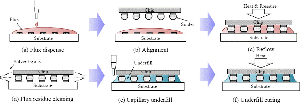
The reflow technology, as shown in Fig. 1, that has traditionally been used, has the disadvantages of multiple steps, difficulty in coping with fine pitch, and severe warpage of fabricated modules. The TCB (Thermo- Compression Bonding)-NCP (Non-Conductive Paste) technology, as shown in Fig. 2, which has recently begun to be partly in production, has the disadvantage of low productivity, still with warpage of fabricated modules, and unsuitable for large devices. The TCB-NCF (Non-Conductive Film) technology, as shown in Fig. 3, which is applied to TSV-based three-dimensional memory production, still has the warpage problem of the fabricated modules, and the productivity is much lower than that of the conventional reflow process. Table 1 compares the features of each bonding technology.


Table┬Ā1
Feature summary of typical bonding technologies
| Items | Reflow Process | TCB-NCP | TCB-NCF |
|---|---|---|---|
| Productivity | O | X | X |
| Warpage | X | Δ | Δ |
| Fine-pitch | X | Δ | O |
This paper introduces laser-assisted bonding (LAB) and its bonding materials as one of technical alternatives to solving these problems. The LAB features vertical thermal gradients between the device and the substrate during the bonding process, effectively reducing the warpage generated by conventional bonding process1). Its short process time provides a good solution to ultra-fine pitch joining as well as ensuring mass production. LAB materials that do not require cleaning, maximize the benefits of LAB. We will use some specific examples to demonstrate the benefits of LAB as a next-generation bonding technology.
2. Laser-Assisted Bonding (LAB) and its bonding materials
The key characteristics of the conventional laser soldering are pinpoint heat and direct contact of laser with the soldering area. Therefore, it was difficult to apply the laser soldering to the bonding of BGA packages on substrates because the laser cannot strike the balls beneath the packages. The laser scans a low of package leads, and its productivity is not so good compared with the reflow process.
One the other hand, Laser Assisted Bonding (LAB) features indirect contact between the laser, and soldering area and homogenized beam, that is, the two-dimensional beam, not a point beam. Laser is irradiated on devices or packages, a portion of laser is absorbed, and their temperatures are increased because of the absorbed laser. Once the devices or packages are heated up, the temperature of the joining areas located beneath the components, also, rises because of the thermal conductivity of the components. The increased temperature of the joining area leads to the bonding process. The temperature of a substrate is maintained close to that of the stage at a bonding equipment. Therefore, the temperature of devices or packages is high compared with that of a substrate. That is, we can obtain the vertical temperature distributions during the LAB bonding process1).
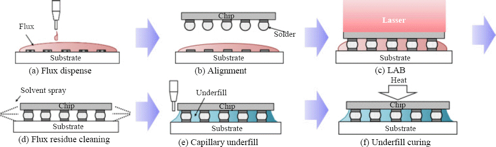
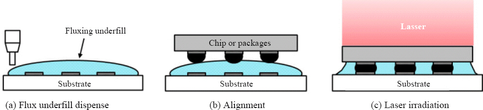
Ordinarily, the coefficient of thermal expansions (CTE) of devices or packages are larger than that of substrates. We have severe warpage problems during the conventional reflow process because of the CTE differences between the components and substrates. However, LAB process can assist reducing the warpage during the bonding process because of the vertical temperature gradients as mentioned above. Additionally, the irradiation time of laser during the LAB bonding process is very short, from less than 1sec. to 10 sec. depending on the application area. It means the productivity of the LAB bonding process is much higher than the conventional reflow process which takes more than 3 min. Fig. 4 shows the LAB process adopted in the current industry. The materials, used in the conventional reflow process, are also applied: flux and underfill. Since the increase rate of the temperature of joining area during the LAB bonding process is so high, compared with the convention reflow process, a suitable material, especially flux, should be developed.
We developed bonding materials suitable for the LAB bonding process2-20). All components, used in the materials are based on polymers. That is, base materials, reducing agents, curing agents, and additives in these materials are based on polymers. Any solvents or conventional flux components are not included. This is important because it is an environmentally friendly process that does not generate gas during the bonding process and does not require a cleaning process after the process. This is crucial for the devices or packages with the high density and fine-pitch interconnection, since the underfill process using capillary phenomena for such components is often not possible.
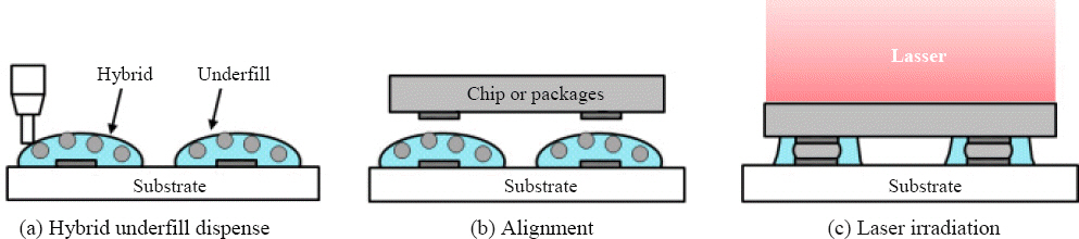
We developed two types of bonding materials for the LAB process; fluxing underfill (FU) and hybrid underfill (HU) as shown in Fig. 5 and Fig. 6., respectively. Fluxing underfill is a kind of NCP (non-conductive paste) and composed of polymer materials. It is designed for the devices or packages with solder balls or bumps. Hybrid underfill includes solder powder which is available commercially. It is designed for the devices or packages without solder balls or bumps, such as passive devices like MLCC, mini LED, and so on. Table 2 summarizes the characteristics of fluxing and hybrid underfills.
Table┬Ā2
Summary of fluxing and hybrid underfills
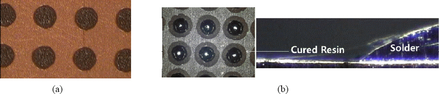
Fig. 7 (a) and (b) show the printed HU on a PCB substrate with Cu finish, and the top and cross-sectional optical images of HU after the LAB process, respectively. The irradiation time of laser during the LAB was only 3 seconds. During the process time, solder powder aggregates to form a solid solder bump. Polymers between solder power are squeezed out and surround the solder bump. Such resin surrounding the solder interconnections enhances the adhesion strength which is important for miniaturized devices. More importantly, this resin prevents solder bumps from bridging each other when bonding devices with very fine-pitch.
3. Applications of LAB-FU and LAB-HU processes
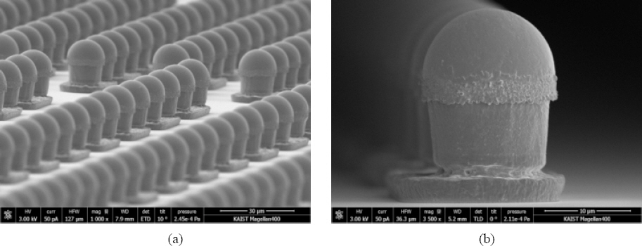
Fig. 8 shows the application of the LAB with FU for the development of bonding process of the daisy chain chip with fine-pitch interconnections. Table 3 shows the specifications of the daisy chain chips. Fig. 8 shows the SEM image of an array Cu pillar/solder cap on a top chip, and a Cu pillar/solder cap, respectively. There was 2ŃÄø-thick Ni layer to obtain long-term reliability under the environment reliability test. The bump pitch of each bump was designed from about 70ŃÄø to 30ŃÄø. The diameter of the bump was designed 18ŃÄø. We applied FU on a silicon substrate with UBMs (Under Bump Metal- lization), and performed a pick and place process using the top daisy chain as shown in Fig. 8. Then, laser was irradiated on the top daisy chain chip. The irradiation time was 2 sec. There was no cleaning process, as mentioned before. Only post curing process was applied to cure the FU between two chips. After finishing the bonding process, we observed the microstructure of the solder joint using the cross-sectional SEM, as shown in Fig. 9. We measured the thickness of the intermetallic compound (IMC) between Ni and solder in the Cu pillar. The thickness of the IMC was only 432nm, which was quite small compared the IMC thickness formed using the conventional reflow process. These phenomena were caused by that the time above the liquidus temperature of solder was maintained very short under the LAB bonding process. In fact, the dwelling time above the liquidus temperature of solder in the conventional reflow process is ordinarily longer than 10 sec., so that there is much time for the diffusion process to form IMC between solder, Cu and Ni.
Fig.┬Ā8
(a) Printed HU on Cu substrate (b) top and cross-sectional optical images of HU after LAB process
Table┬Ā3
Specifications of daisy chain test vehicles
| Type | Dimensions | Surface finish of pads | # of pads |
|---|---|---|---|
| Top | 11├Ś7├Ś0.78mm3 | Cu pillar/Ni/SnAg | 27,000 |
| Bottom | 13├Ś8.5├Ś0.78mm3 | Ni/Au |
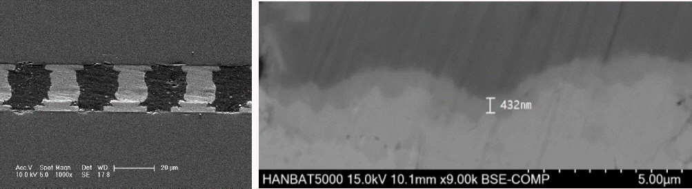
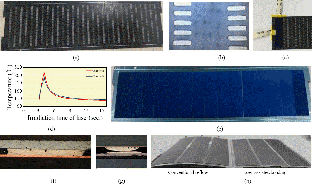
Fig. 10 shows the application of the LAB with HU for the development of back-contacted Si solar cell array on a PCB substrate. Fig.10 (a) and (b) show photographs of a PCB substrate and printed HU on a PCB, respectively. To establish the process conditions of the LAB bonding, a thermocouple was positioned between a solder cell and a PCB substrate, as shown in Fig. 10 (c). With adjusting laser power, a suitable condition was obtained as shown in Fig. 10 (d). The irradiation time was 3 sec. Fig.10 (e) shows a mounted Si solar cell array on a PCB substrate. Using LAB and HU, there was no open defect as shown in Fig. 10. (g), which was observed when the conventional reflow process was applied. All joints exhibited good interconnections, as shown in Fig. 10. (f). The comparison of Si solar modules fabricated using the reflow and LAB, respectively, was shown in Fig. 10. (h). The amount of warpage was greatly reduced using the LAB process, compared with that using the conventional reflow, which was a major reason why the open fault disappeared with the LAB process.
Fig.┬Ā10
(a) PCB substrate for solar module, (b) printed HU on PCB substrate, (c) thermocouple between solar cell and substrate, (d) meausred temperature profile during laser irradiation, (e) mounted Si solar cell on PCB substrate, (f) good interconnection when LAB process is applied, (g) open faults observed when reflow process is applied, and (h) warpage comparion of modulle faricated using conventional reflow and LAB with HU
4. Conclusions
Laser-Assisted Bonding (LAB), fluxing and hybrid underfill materials were introduced. All components included in the two materials are based on polymers so that there are no underfill and cleaning process when the materials are used, which makes the LAB process more attractive. We showed two applications using the LAB with the two materials: Bonding of daisy chain chip with fine-pitch interconnection and back-contacted Si solar cells on a PCB substrate. The IMC thickness of the microstructures in the solder joints in the daisy chain was very small compared with the conventional reflow process because its very short dwelling time above the liquidus of the solder material. The LAB with HU made the amount of the warpage of the solder module decreased becaue of its vertical temperature gradient.
 PDF Links
 PubReader
 ePub Link
 Full text via DOI
 Download Citation
 Print
Print